Hello friends, I hope you all are doing great. In today’s tutorial, we will have a look at the Common Base Amplifier. The common base amplifier configuration is also called a grounded base is a basic single-stage amplifier configuration of BJT like a common collector and common emitter amplifier. This configuration is normally used in the current buffer or voltage amplifiers circuits.
In this circuit, arrangement emitter operates as an input collector as output and base are attached to the ground or as a common point. In today’s post, we will have a detailed look at its circuit, working and some other parameters. So let’s get started with Common Base Amplifier.
Common Base Amplifier Circuit
- In common base amplifier circuit arrangement, the emitter is operated as input, a collector as output and base is common to point for both emitter and collector.
- The other names for this configuration are CB amplifier or CB configuration.
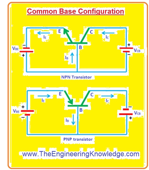
- For this circuit input voltage is given among base and emitter points and output is taken at collector and base terminals.

- From this, you can note that base is common to point for emitter and collector due to that it known as the common base configuration.
- The voltage given to the terminal base and emitter is denoted as VBE and voltage among collector and base denoted as VCB.
- In this configuration like other arrangements base-emitter junction is forward biased and collector-base junction is in reverse-biased condition.
- In the below figure common base amplifier circuit is shown for both NPN and PNP transistors.
- You can see from the above figure that input is given at emitter and output is at collector and base is a common point.
Current Flow in Common Base Amplifier
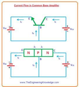
- For understanding let’s take NPN transistor as a common base amplifier.
- In the figure you can see that base-emitter junction is in forward biased condition through applied voltage VBE and collector-base junction is in the reverse-biased state through thee voltage source VCB.
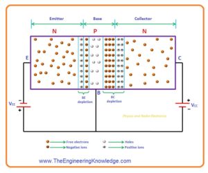
- Due to forward biasing voltage VBE electrons that are major carriers in emitter will bear a force of repulsion due to the negative terminal of the battery also holes in the base of the transistor will bear the force of repulsion from the positive side of the voltage source.
- Due to this electrons move toward the base from the emitter and holes move from base to emitter.
- Due to the movement of electrons and holes current flows. The real current is due to the flow of electrons which flows from emitter to base.
- But we follow conventional current that is from base to emitter. Hence current is generated at base and emitter.
- The electrons that move from emitter toward base will combine with a hole which is majority carriers and holes moving toward the base to emitter combine with the emitter.
- In the above diagram, you can note that the area of the base is very less. So less number of electrons coming from emitter will combine with holes in base remaining will enter to the collector.
- The electrons enter into the collector will bear the force of attraction from the positive side of the battery.
- So free electrons in collectors move to the positive side of the battery due to that current is generated at the collector region.
- The current produced at collectors and base is due to electrons coming from the emitter. hence, emitter current is large than the collector and base current and equal to the sum of these two currents.
IE = IB + IC
- As we discuss above emitter is input and collector is output.
- As output or collector current is less than the emitter current hence gain of current is less than the one.
- In simple words, a common base amplifier attenuates current that amplification of it.
- As the base-emitter junctions at input operate as a forward-biased diode. So the impedance of a common base amplifier at the input is less.
- The collector-base junction behaves like a reverse-biased diode due to this impedance for a common base at the output is high.
- So we can conclude that input impedance for the common base is less and high at the output.
- Such a transistor that has less input impedance and large output impedance give large voltage gain.
- As the gain is large but the current is less so the power gain of this amplifier is less than other amplifiers.
- These amplifiers are used in such an application where less input is needed.
- Base amplifier configuration is mostly used in the current buffer circuit.
- This amplifier is not commonly used as a common emitter and collector is used.
Common Base Amplifier Input characteristics
- The input characteristics define the relationships among the input resistance IE and input voltage VBE.
- For explanation draw x and y-axis and input current which is emitter current draw on the y-axis and input voltage VBE on the x-axis.
- To calculate input parameter output voltage which is VCB keeps constant at 0 volts input voltage increases from 0 to different voltage values.
- For every value of input voltage VBE, the value of input current is measured.
- In below figure graphical representation among the input current IE and input voltage VBE at constant output voltage or zero volts.
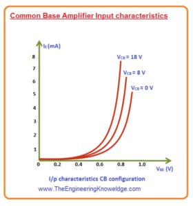
- After that output voltage 0 to eight volts and keep constant at eight volts.
- During increment in output volts, the input is constant at 0 volts.
- After this output voltage is constant at eight volts the input VBE increases from 0 to different values.
- For every value of input voltage, the input current is measured.
- The graphical representation constructed among the input current and input voltage at eight volts output..
- This is repeated for higher fixed values of the output voltage (VCB).
Common Base Amplifier output characteristics
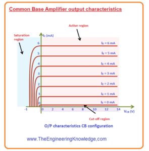
- The relation between the collector current and the output voltage is defined by the characteristic curve.
- The output current is drawn on the Y-axis and output voltage on the X-axis.
- For the determination of output parameters, the input current is remains constant at 0 volts and the output voltage increases from 0 to different values.
- For every value of output voltage, the output current is measured.
- The graph is constructed among the output current and output voltage at constant input current IE or 0 milliampere.
- When the emitter current is zero transistors is operating in cut off region.
- After that value of the input current is increased from zero to one milliampere by varying the input voltage VBE and input current is constant at one milliampere.
- During the increment in input current IE the output voltage VCB is constant.
- After that input current is constant at one milliampere output voltage is increases from 0 to different voltage values.
- For every value of output voltage, the output current value is measured.
- The curve is then constructed between output current IC and output voltage VCB at constant input current one milliampere. This region is called active region of a transistor.
- This process is repeated for large values of current 2,3, 4, and so on milliamperes.
Read also
- Common Source JFET Amplifier
- Common-Gate FET Amplifiers
- Common-Source FET Amplifiers Operation
- Common Collector Amplifier
- Common Emitter Amplifier
So friends it si detailed post about common base amplifier if you have any question ask in comments. Thanks for reading/

