 Hello friends, I hope you all are doing great. In today’s tutorial, we will have a look at the Common collector Amplifier configuration and its applications. It is another category of BJT amplifier configuration in which input voltage is given at the base and output is taken at the emitter of the transistor. While collector is common between base and emitter terminals.
Such type of arrangement is known as a common collector because the collector is linked with the ground. In today’s post, we will have a detailed look at its circuit and some other related parameters. So let’s get started with Common Collector Amplifier.
Common Collector Amplifier
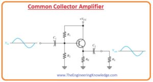
- In below figure a circuit with voltage divider bias configuration is shown. This circuit is followed by the circuit used in common emitter configuration that we have discussed in the previous tutorial.
- You can see that input voltage is coupled with the base through the capacitor and collector is ground.
- The output signal is not inverted than the input signal but in same in magnitude to input.
Common Collector Amplifier Voltage Gain
- As we know in all amplifiers the voltage gain is Av=Vout/Vin.
- The capacitive reactance will be ignored at frequency operation.
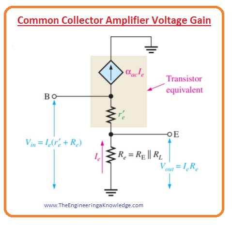
- In below figure ac model is shown.
Vout=IeRe
Vin=Ie(r’e+Re)
- So the voltage gain equation will be.
Av=IeRe/Ie(r’e+Re)
- The base emitter gain expression will be as.
Av=Re/(r’e+Re)
- In this equation, Re is in parallel with the RE and RL. If a load is not connected then Re=RE.
- You can notice that gain is always less than the one.
- If Re>>r’e then the fine estimation will be.
Av=1
- As the output voltage is across the emitter it phase is similar to base voltage due to that there is no inversion occur from input to output.
- As there is no inversion at output as voltage gain is almost one the output voltage is the same as input for both phase and magnitude.
Common Collector Amplifier Input Resistance
- The input resistance for this common collector circuit is large.
- Due to large input resistance, it can be used as a buffer to reduce the loading effect. When the circuitry is running a load of less resistance.
- The calculation of input resistance observing from the base of the common-collector amplifier is like the common emitter amplifier which we discuss in the previous post.
- In common collector, though the emitter is never bypassed since the is taken about Re that is RE in parallel with the resistance RL.
Rin(base)=Vin/Iin=Vb/Ib
=Ie(r’e+Re)/Ib
As Ie=Ic=βacIb
Rin(base)=βacIb(r’e+Re)/Ib
- So we have after simplication.
Rin(base)=βac(r’e+Re)
- If Re>>r’e then the input resistance at base is after simplification.
Rin(base)=βacRe
- The bias resistance shown in the first figure is a parallel with the Rin(base) observing from the input like common emitter input resistance for a common collector is.
Rin(tot)=R1ІІR2ІІRin(base)
Output Resistance
- If load is not connected the output resistance will be given as.
Rout=(Rs/βac)ІІRE
- In this equation, Rs is the input resistance of the source
Current Gain
- The current for a common collector is given as.
Ai=Ie/Iin
- In this Iin is equal to the Vin/Rin(tot).
Power Gain
- The power gain is the product of current gain and voltage gain.
- For common-emitter power, the gain is one since voltage and current gain almost equal to each other.
- As Av=1 the power gain is
Ap=Ai
FAQS
What is a common collector amplifier?
- The common collector amplifier is 3 single-stage bipolar junction that amplifies circuits that are used for voltage buffers.
Why is it called a common collector?
- It is called a common collector since both signal source and load share collector have a common collection point. Input is provided at the base and collector.
What are the features of a CC amplifier?
- The common collector amplifier is defined as an emitter follower normally as a voltage follower. The main features for voltage follower are high input impedance, low output impedance, and noninverting voltage is 1.
What is the working principle of CC configuration?
- In this circuit, input is given between the base and collector and output is taken between emitter and collector. The collector of a transistor is common for input and output circuits and is known as a common collector connection.
What are the applications of CC amplifier?
- This amplifier circuit is used as an impedance-matching circuit. it is also used for switching modules.
- The high current gain configured with unity voltage gain makes that circuit good voltage buffer.
- It is also part of circuit isolation.
What are the advantages of common collector configuration?
- It comes with a high current gain, voltage gain is less than unity.
- it has lower output resistance than other amplifiers.
- It is also called an isolation amplifier.
Why does a common collector have high input impedance?
- The input impedance is high for the common collector since measured with the Beta of a transistor, taken product of emitter resistance. The current gain is due to output impedance inverse proportional to the current gain of the transistor in parallel to R.
Read also:
so, friends, it is a detailed post about the common collector amplifier if you have any post ask in the comments. Thanks for reading. Have a good day.


