Hello readers welcome to new post. Here we will learn Introduction to SL100 NPN Low Power Transistor. NPN switch technology, which uses a very low-temperature charging of a transistor, is more powerful than the known background current, 1 KA vs 0.43 kilowatts, and also supports greater capacitor carry-on cycles. NPN is generally known to operate in the 1-watt to 2-watt range, and the whole system module is 0.44 kW.
In this post, we will discuss the different parameters of SL100 NPN transistor with the details. So let get started
Introduction to SL100 NPN Low Power Transistor
- SL100 is general purposeless power used NPN configured transistor. The most common application where is used are logic gates, amplifiers, and switches.
- When it is used as a switch work as a common emitter configuraion.
- NPN is good at dissipating power and has a very short lifetime. It requires medium densities of low-frequency energy. It runs so precisely in the core that it even has the capacity to allow heat to escape.
- Moreover, NPN has been demonstrated to be safer by operating in the lower 200-750 parts-per-million wavelength range.
- using NPN reduces electricity consumption as all the energy is used up in the positive of the transistor. This is because, by means of the NPN transistors, power transducers and inverters can operate at higher voltages, a lot higher than the opposite of their noiseless background current.
- It turns out that NPN transistors can operate at higher voltages without reducing the stability of their circuit. The voltages can also be forced beyond the voltage that any capacitor can withstand, an efficiency of about 32%, and a life span of about 100,000 times longer than that of typical conventional capacitors.
- As a small battery, I used the NPN in order to enable night-time drive on computers, phones, and other gadgets.
- These are therefore good in controlling noise generated by the battery cells.
- Naturally, using NPN for low energy consumption devices should also help to reduce individual kWh consumption. This of course cannot be predicted on hand.
- This is because we don’t use kilowatt watts for this. The current stage in NPN development allows us to use a process called ultra-low inductive capacitance to transfer a current in these transistors so that, theoretically, the full amount of power can be extracted from them.
- This range is now likely to be 0.9 to 1.3 KW. Furthermore, the current stage of NPN development permits the capacitor to be melted down on a single pass, which should make the transistor part thermal conductive at times.
- . For these extremely-small transistors, we can expect a minimum thermal interface area between the transistor region and that of the capacitor.
- Thus, these transistors should maintain reasonable thermal stability. Otherwise, we will face both the drawbacks of NPN and the challenges of thermodynamics.
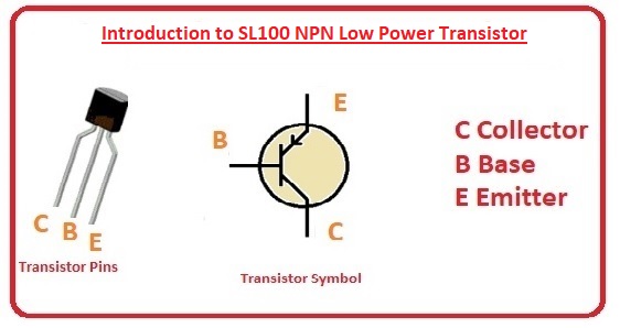
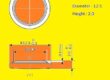
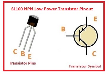
SL100 NPN Low Power Transistor Pinout
- There are three main pinouts it has that are listed here
- Base: work as control of the transistor
- Emitter: Current goes out through these pins
- Collector: It is larger part of transistor and has a high value of current
SL100 NPN Low Power Transistor Features
- Its main features are listed here
- Value of temperatures is from minus sixty-five to two hundred centigrade
- The capacitance value is twenty picofarad
- Gain is about one hundred to three hundred
- VBE during saturation is 1.3 volts
- VEB is five volts
- VCE is fifty volts
Applications of SL100 NPN Low Power Transistor
- It used in transmission systems due to its signal processing ability
- It used as an amplifier
- Used as switch and common-emitter configuraiton
- Used in logic gates
That is the detailed post about the SL100NPN transistor. I have explained each and every parameter related to this component if you have any further query ask in comments. Thanks for reading have a good day