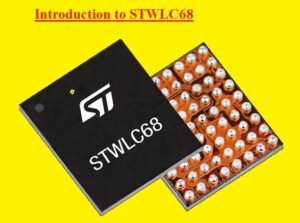
 Hello readers welcome to new post. We will cover the details of Introduction to STWLC68. it is used for different small-level devices and can work on the five-watt output power supply and is called an integrated wireless power receiver. It is compatible with Qi 1.2.4 features to perform the inductive communication protocol.
Its efficiency is good and it is credited to less loss synchronous rectifier and fewer losses linear regulator. In this post, we will cover its details working features and some other paramerts. So let’s get started with Introduction to STWLC68.
Introduction to STWLC68
- STWLC68 module is created by STMicroelectronics that is a group of different wireless charging integrated circuits.
- This manufacturer give the different wireless devices that give the solution to the industry like high efficiency, high power transfer, and protection.
- These new modules enhance the rapid power transfer and power delivery to different devices.
- With the use of I2C intefacing users can get and modification of different structures.
- The configured details can be save in the embedded OTP memory unit and than get automatically through power up permitting this component to operate as a standalone module
- It comes in chip scale packaging
- It has less value of impedance high volts synchronous rectifier and less loss regulator.
- It needs less value of bill of material are considered as the finest option for small power users applications like mobile phones and tablets
STWLC68 Features
- Its main features are discussed here
- Its chip scale packaging increases the power dissipation
- It has features to protect the over volts and over current conditions
- It has I2C interfacing with the frequency of four kilohertz
- It has a configuration of over volts clamping protection
- It measures the correct value of current and volts for FOD devices
- It consists of six general-purpose inputs and outputs
- It has eight changes ten bit analog to digital converter
- For data configuration, it has OTP memory unit
- It has an ARM cortex microcontroller with features of thirty two-bit and sixty-four megahertz
- It has 3.6 volts to twenty volts programmable outputs
- Its output power is five watts
- It is compatible to Q1 1.2.4 inductive wireless communication protocol
STWLC68 Applications
- STWLC68 Applications are explained here
- It used in different wearable modules
- Used in medical devices
- used in GPS systems’
- Employed in power banks
- Used in mobile phones and tablets
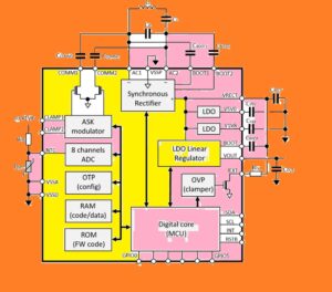
STWLC68 Block Diagram

STWLC68 I2C interface
- The STWLC68 can function without the use of any interfacing like a controller. For such applications where STWLC68 is connected to main parts controlled through the host then two pinout SCL and SDA can be interfaced to the I2C protocol
- It operates as a salve of I2C protocol and is compatible to standard and high-speed transfer of data that is one hundred Kbits/s for standard and 400Kbits/s for high-speed
- With the use of I2C interfacing, the extremely flexible operation can get and it also made possible to connect to internal structures.
- The host regulation helps to show the status of the module transfer of power
Read also
- Comprehensive Guide to PCB Voltage Regulators: Types and Applications
- What is Voltage Regulator, Types and Working
- What Function Does A Proportional Pressure Regulator Serve?
- Why is My Water Heater’s Relief Valve Leaking?
That is all about the STWLC68 all details are discussed if you want to get more ask in the comments. Thanks for reading have a nice day


