Hi, readers welcome to another interesting. In this post, we will have a detailed look at the Introduction to 74LS74 Dual D Flip-Flip flop. This category of flip flop compromise of Schottky transistor transistor logic circuits configuration which helps to the production of D type flip flops having high speed. The flip flop used in this board has its own discrete inputs pinouts and with that also has discrete outputs Q and Q’.
The main and common usage of flip-flops in digital electronics in different categories of circuits and devices. in this post, we will cover its working, pinout datasheet and some other features. So let’s get started with Introduction to 74LS74 Dual D Flip-Flop.
Introduction to 74LS74 Dual D Flip-Flop
- The IC 74LS74 is the double D type edge-triggered category of flip flops comprise of clear preset and complementary output terminals.
- It has the ability to store data in the form of binary numbers and it also comes with features that stored data can be changed when required.
- It offers specifications of the high value of operating voltage, different functioning requirements, and provides a facility to make a direct link to the CMOS, TTL, and NMOS.
- The low level that exists at the preset input terminal helps to reset set the output value according to the logic levels of the provided inputs.
- This category of D flip flop also called data or delay flip flops. This module provides features to get the value of D input at a certain part off the signal or clock cycle like at the falling edge of the clock signal.
- The data at the D input is get through the flip flops at the positive end of the pulse.
74LS74 Features
- The main features of 74Ls74 are described here with the details.
- The value of temperature over which it operates is two volts to fifteen volts.
- The value of propagation delay for this device is forty nanoseconds.
- It available in the dual D flip flop packaging integrated circuit configuration.
- The value of the minimum high-level input voltage for this module is two volts.
- This flip flop comes in So 14 packing and has fourteen pinouts.
- The value of temperature over which it operates is zero to seventy degrees.
- The value of the maximum low-level input voltage for this board is 0.8 volts.
- The high-level output current value is eight amperes.
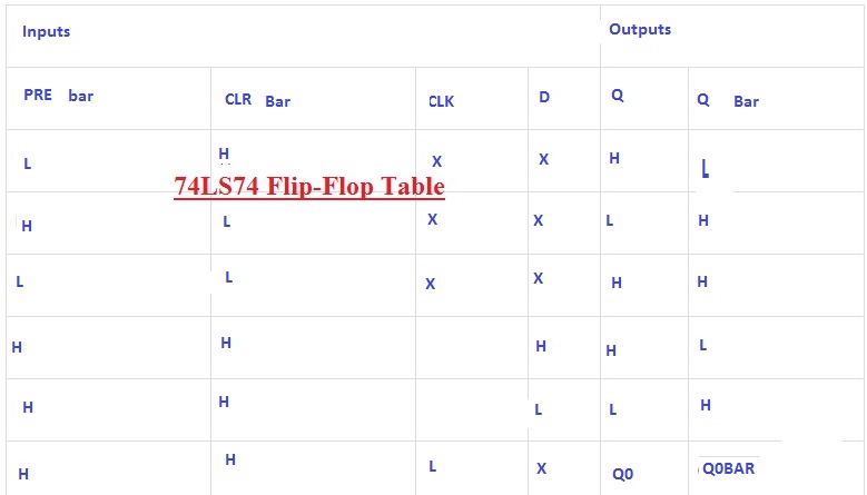
74LS74 Flip-Flop Table
- Here you can see the table of 74LS74 flip flop.
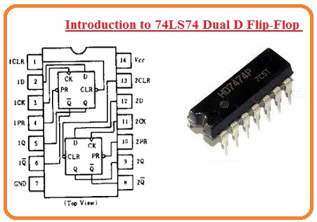
74LS74 Flip-Flop Pinouts
- Fourteen pinouts of this board are described here with the details.
- 1Q / 2Q: It is the output terminal of this board.
- 1Q’(bar) / 2Q’(bar: this pinout no six and eight and inverted pinout and called complementarily.
- 1CLK / 2CLK: At this pinout, a clock pulse is provided and are number three and eleven.
- 1CLR (bar) / 2CLR (bar): these pins are used to clear data and are reset pinout and their number is one and thirteen.
- 1D /2D: Through these pinouts, data is provided to the flip flop and their number is two and twelve.
- 1PRE (bar) / 2PRE (bar): These pinouts are used as inputs for flip flops and the number is four and ten.
- Vss: It is pinout number seven and is used as ground.
- Vdd/Vcc: it is pinout number fourteen and used to provide five volts to the flip flop.
Applications of 74LS74
- The main applications of this board are described here in the detail.
- It is used in different categories of latching instruments.
- It is the main part of buffer circuits.
- It is used in memory units.
- Used in Tvs
- It is part of notebooks and a personal computer
- Commonly used in digital electronics and networking instruments
- it is used in sampling circuits.
Working of 74LS74
- The working feature of 74LS74 is simple to give power to IC through Vcc and ground pins. Each flip-flop works independently. Make the connection of input signals with pins 2 and 3 for handling flip flops with output given at pins 5 and 6.
- Pin 3 needed a clock signal normally a PWM signal from MCU or we can give it through 555 timer. THe pin activation to high conditions clear date and reset flip flop.

Why is D flip-flop better
- D flip flop is more significant than other types of flip flops. It makes sure that both inputs S and R will never have one value. Gated flip flops are used to design delay flip flops having an inverted connection between inputs.
What are the 4 types of flip-flops?
- S-R Flip Flop.
- J-K Flip Flop.
- T Flip Flop.
- D Flip Flop.
How many D flip flops are there in a 7474 IC
- It has four d flip flops
What does the triangle on the 74ls74 mean?
- Triangle explains that a clock signal is edge triggered signal
- The circle defines that signal is low active.
Read also
- What are the Types of Integrated Circuit (IC)?
- How is a Microprocessor Different from an Integrated Circuit
- Introduction to Integrated Circuits (ICs)
- Latch Circuit using 555 Timer
FAQS
How many flip-flops are in 74LS74?
- This ic comes with two separate D flip flops that activated on a positive edge and provide reverse output results
What does the triangle mean on 74LS74?
- The triangle shows that the clock signal is edge triggered and the circle defines that the signal is active low
What is the main use of a 74LS74?
- The IC 74LS74 stores data in binary numbers and also has features that help to change data saved if needed
What is the D flip flop using 7474?
- Edge transition activates 7474 ICs the variations to Q output occur if there is a shift at input trigger features. The triangle at the clock input defines its activation for rising edge.
What are the 4 types of flip-flops?
- Latch or Set-Reset flip-flop.
- JK flip-flop.
- T flip-flop.
- D (Delay or Data) flip-flop.
What is the difference between D and T flip-flop?
- For clock signal flip lop gets and saves the value shown at D input of D flip flop.
- While for T flip flop, clock pulse, the stored value in flip flop either switches or remains constant according to T input either 1 or 0.
What is D flip-flop truth table?
- The D flip flop is important for different clock types. It makes sure that two inputs S and R not same time set 1. The delay flip flop is made with the use of a gated SR flip flop where the inverter joins inputs to enable the singular D(Data) input.
| CLK | D | Q(n+1) | State |
| – | 0 | 0 | RESET |
| – | 1 | 1 | SET |
So friends that is a detailed post about 74LS74 I tried to cover each and every aspect related to this device. If you have any further queries ask in the comments. Thanks for reading. Have a nice day.