 Hello readers welcome to new post. Here we will discuss Top PCB Inspection Techniques. PCB is very significant part of any electronic project and device that commonly used. PCB is comes with conductive layer where different symbolic representation are designed to connect the different components for projects creation.
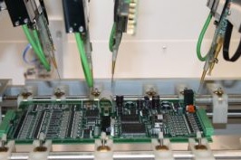
There are different techniques are used for the creation of accurate PCB designs and projects. These methods help us to make our project very accurate and fine. These testing tools helps us to know about the quality of our products created whether it are created according to our requirements or not. There are different PCB manufacturers and suppliers that are offering PCB testing services with different features but PCBWAY is the best in all not only offered PCB manufacturing services but as well PCB testing modules with good quality machines.
Top PCB Inspection Techniques
- Commonly used PCB inspection techniques are described here.
In-Circuit Testing Technique
- This testing techniques is very commonly used test. In this techniques open circuit test, short circuit paraments of components and function of integrated measured and also named as capacitance test.
- In this test technique
- This circuit device comprises of pins that connect at the different points and resistance is measured.
- The pins finds the connection of solder board points. For initiating the test press the board at the areas of probes.
- PCB creators do this test at the mature modules which have finest structure.

Automated Optical Inspection (AOI)
- AOI is an automatic test that gives high degrees of fault detection speed and repetition that not occur for manual processes.
- There is two dimensional and three-dimensional camera is used to make pics that are compared with the original structure.
- If there is no matching between the structure and pics then the layout will be changed.
- This test is considered as finest when used it at the end of a soldered board construction line. Through this solders defects can be found.

PCB Testing Service Provider
- There are different PCB testing service providers working in the world that offer different services at different rates. PCBWAY is a best service provider that not only provides the PCB manufacturer services
- As part of our ISO9001: 2008 quality management system PCBWAY undertakes three phases of PCB testing for all pre-PCB testing and performance testing operations Before we leave our factory, all parts of the board require rigorous testing.
- PCBWAY offered the PCB Function Tests and Services
- 1. Visual inspection after the SMD Process
- 2. Free AOI Testing
- 3. X-ray Testing for BGA package, Function Testing, etc with extra charges.
- 4. Final visual inspection
- PCBWay can provide you with a functional test (FCT) for your boards. Functional testing ensures that the PCBs found are in working condition.
- Functional testing is usually done after circuit boards are assembled and AOI and visual inspections are completed. Preliminary testing allows us to detect and repair structural defects, organizational defects or design problems that may occur early and to resolve the problem as quickly as possible.
- PCBWAY is one of the best in all features and other services that you want to avail must contact them their engineers will guide you to get good services at reasonable rates and prices.
Flying Probe Test
- This test helps to finds the diode’s inductance resistance short circuits and open circuits. In this test there is probes used and connected to the X-Y grid needle.
- The basic difference between a flying probe and in in-circuit test is the starting price.
- Though ICT is a high-speed test and has less chance of faults. ICT can be less expensive in case of bulk orders then the flying probe.

X-Ray Inspection
- It is used in different electronic industries. Through observing the solder connections barrels and inner traces faults can be measured.
- These tests perform in three dimensions and two dimensions way.
- This test helps to find the defects for such points that are not easy to trace such as in ball grid packages solder point that are not easy to approach.

Functional Test
- This test is used for checking the product power-up. It needed different features and exterior devices. It should fulfill the UL and MSHA standards.
- Users normally send the details of functional tests and different parameters and creators give details to create and make the product.
Burn-in Test
- It is used to find the detection of initial damages. Its intensity can damage the other parts. It runs power through the board regularly.
- This test is normally used for medical instruments and applications.
That is all about the Top PCB Inspection Techniques. The different test have been described here with the details if you have any further queries ask in the comments. Thanks for reading have a nice day.Read our More Engineering Blogs


