Hello, readers welcome to the new post. In this post, we will discuss Ordering Instructions at JLCPCB. JLCPCB Established in 2006, JLCPCB is a famous board company. It comes with more than 15 years of innovation and good customer requirements company and it growing fastly world-famous supplier of boards with low-cost boards making it famous in the industry.
It provides high quality and growth for PCB technology and helps to provide a highly accurate board that is used for industries, aviation industry, and medical projects.
In this post, we will define details that user faces for placing orders on JLCPCB for their product and different services. There are some functions performed by JLCPCB in order to minimize any problems. Here are some guidelines that help before placing any order on JLCPCB. So let’s get started
Ordering Instructions at JLCPCB
- First of all, we discussed instructions for PCB orders and then instructions for stencil order
Instructions for PCB orders
Solder-resistance bridges
- For solder resistance, bridges spaces between pads are about 0.254mm, and special measures are considered for solder mask bridges.
Proper English descriptions and other attachments in the zip file
- There is no need for English details and other descriptions for Zip files like PDF files and Excel DXF, and board production is performed based on the Gerber file that is sent must work on a clear and good Gerber file.
- Make sure that the correct values are provided for the Gerber file and if there are any more points added in detail before placing.
PCB file and GERBER file in the zip file at the same time
- If you send board files and Gerber files in Zip will use the Gerber file and ignore the PCB files
Plated edges/ slots Dimensions
- If there need for edge plating or plated slots, then define a length not higher than 6mm and also note it before ordering or they not make it. If there are details about it then they make it in the normal process.

Problems related to software incompatibility
- Some different users employ different software for board designing and the software that JLPCB uses for the Gerber data process is not like as software used for a design that resulted in software incompetency.
- As there is no warning related to problems at the time of data important in software, they do not come with any method for noticing and do not confirm it with users, so they are responsible for half of the order issues related to software incompatibility
Markings on base materials
- Due to security issues, there are markings on base materials that is according to the base material and do not have a technique for removing it. They do not come with an idea about which board comes with the type of marking, so some boards come with a chance of being marked. Make sure that is the reason before order placement
Designs about slots/CUT OUT/ millings/ v-cut
- Make sure that there are V cut lines, cutouts, milling, and slots for the same layers having a routine of the board. If it does not exist in the same layers as with the routine of the board, it will be missed. Check it before placing an order. If it is issued due to their not like same layers with the board outline, JLCPCB will not be responsible for it.
4 Layer PCB
- Normally they do not make 3 layers of the board if your order is 4 layers and the other is single inner layers, they will process with 4 layers and make sure again. Check either is any inner layers not exist or not when the orderis placed
About repeat order
- Generally, order repetition is produced based on the production file of previous orders and will not make any changes to the production file. So ensure that not leave any notes based on order variation when placing orders. The repeat order will not be manually checked with their engineers
- Note: The engineering fee will still be charged by the system since our engineers need to re-penalize the boards manually.
About the items in the board outline
- The board outline is for showing what your baord looks like when it is completed. So all these that are needed for cutting with plate outline must added for the plate outline layers, like cut lines, grooves, milling, and cutouts.
- To remove unnecessary for avoid any confusion, note that if there is both GKO layers and GM1 layers in the Gerber file, theri engineering ignores GKO layers and makes a board based on GM1 layers.
- If there is GM1, GM2 or GM2, GM3, and GM4 layers in the Gerber file at the same time they use one with small number after the letter GM for the cutout layer with default. Such as if there are GM2, GM3, and GM4 layers in the Gerber file, we will follow GM2 as the contour layer and ignore GM3 and GM4.
file generated from EasyEDA
- Easyeda is free online software that they provide for PCB desing and you can place an order on JLCPCB easily and fastly. But if there is manufacturer errors due to desing errors they will not be responsible for it
About JLCPCB panel
- Normally if you select the JLCPCB for a panel of PCB during order placing, generally they will panel your order with V cut in rectangular and round shapes only. If you have a panelized board yourself but select the one pcb during the order placing some desing in the Gerber file must not be more than five, then they can cancel the order. If the panel by the customer has been a select number of designs in a panelized Gerber file must be not more than ten
Remark field
- There is a note field when you place your order so you can leave a note in case of import, but they do not recommend using this option as all orders with an English note will take longer to go through the audition process.
About the board that is larger than 200mm*250mm
- For a board that is larger than 200 mm*250 mm as there is board is larger and they will try to make it but it good board is not enough for the quantity you order in the website due to huge charges of production, they will send a good board and refund the difference to you
Design about the thickness of board outline /slots/CUT OUT/ millings
- Generally, they suggest that design of 0.15mm for plate outline thickness, slot, cutout, and milling. But if the thickness of the board outline slots cut out, and milling is greater than 0.15 mm, they will follow the center line to make the board outline, cut out, and milling.

About the board within or equal to 50mm*50mm
- For smaller baord that have dimensions 50 mm*50 mm, the size of the board is smaller and it is difficult to mill accurately during the milling process. They suggest that panelize the small board to have fewer problems
Solder mask layer
- A layer of solder mask is a must-have layer. Ensure that you have added it to your Gerber file. If the solder mask layer does not exist or the solder must layer is empty, the board will be created as fully covered with solder mask ink as default. So desing solder makes layer accurate if you have a good solder mask opening. And if you want the complete board to be covered with tin ensure to remark it when order place
Other instructions:
order cancellation
- For orders that are missing some layers, e.g. the board outline and drilling are missing, they will cancel the order directly. If no drill etc. is required, you should note this when placing the order; otherwise, it will be canceled directly during the audit process.
About orders beyond JLCPCB capabilities
- For orders that do not according to the JLCPCB capabilities, they will directly cancel the order and send you an email to inform you of the reason. Before you pay for the order, please check your file carefully to save the loss due to cancellation.
stencil production file
- Generally, you select JLCPCB for the penalization of PCB. If there is no stencil order they will not make a production file for stencil as engineers who make production files do not know how to make a production file for the stencil
About Removing Order Number:
- For these orders, choose the order number removal service or specify the location service, they will usually follow the instructions of the clients when making the boards. Just in case, they also recommend clients to choose a Production Confirmation service that can check it.
Generally, it will not affect the function of the boards if JLCPCB forgets to remove the order number or enter it accidentally, in this case, we will refund the order number removal fee.
Instructions for Stencil ordering at JLCPCB
Stencil thickness
- As there is no option to select the thickness of the stencil on their website and their engineers will choose the thickness for you based on your file. If there is any certain thickness that needs then make a note about it when you place an order
English descriptions and other attachments in the zip file
- There is an English statement or some other descriptions that exist in your zip file like PDF files, or DXF files, Excel, etc that will not be considered and the stencil will be completed based on the Gerber file. If there are certain requirements, then mention in the remark field during order placing
Tooling holes
- If tool holes are required for your order, please make sure the circles are padded in the solder paste layer, otherwise, they will not make it for you.
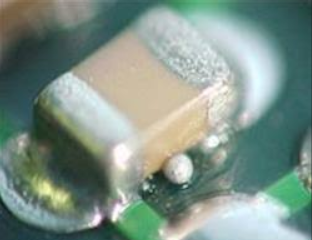
Solder beading treatment
- Solder balls, a defect that can result in short circuits, are generally related to excessive solder paste deposits that, due to the lack of “body”, are compressed under the discrete component and then become a solder ball. The most common place to see solder balls is on the side of chip components such as resistors and capacitors.
- On the JLCPCB, the template hole for components (except the diode) greater than or equal to 0805 will be slightly reduced from the size of the pad as shown below to avoid solder balls.
Note: If you do not wish to use this solder bead modification for your template, please indicate so when placing your order.
About the spacing for different designs in your stencil file
- Generally, if the stencil size is large enough to add different designs to the template, they won’t change the spacing between your designs But if the stencil is not large they set the spacing for these desing that can be added on the stencil. If no variation can be made on the panel make sure to make a note about it during the order placement

Direction of stencil
- Normally if there is no note about the point where to put the cut on the stencil long side of the board will be on the same side as the long side of the stencil automatically
Apertures for through-hole components in the stencil
- The aperture for through-hole elements will not be created by default in the stencil. A special note is needed when the order is placed
Other instruction
Complaints about the re-order
- Please check or test the order when you receive them, if there is any problem, once the problem is confirmed, if it is a problem from JLCPCB, they will offer to refund the order or rework. If there is no feedback and the order is re-ordered, if there is any problem with the order that is ordered for the first time and the order for the new order, we can bear the loss only for the order that is ordered for the first time.


