 Hello, readers welcome to the new post. Here we will discuss the Importance of PCB Production Compensation. When a PCB board is constructed and designed there are some factors such as material features, the process used for construction, and environmental conditions, which can vary in the electrical parameters of the board and affect board operation. So some compensation measured is used to ensure the accuracy and good quality of the board.
Here we will discuss production compensation used by PCBWAY for PCB construction. PCBWay is a manufacturer specializing in PCB prototyping, low-volume production, and PCB Assembly service all under one roof. They provide quick turn boards at low prices. Thousand of engineers, and students are using their boards with their projects.PCBWAY works to be an easy manufacturer for their customers.
The main objective of PCBWAY is to become the world’s number one manufacturer of all types of boards that help to provide you with quality boards at reasonable prices. With that, they are also using the latest instruments and developing technical and management systems for handling flexible machine configurations at production at a few boards without affecting delivery time, cost, and quality. All these factors make PCBWay your one-stop destination for low-cost PCBs.
If you find any defects after receiving your PCBs or are dissatisfied with their products or services, please let them know immediately at [email protected], and they will respond within 24 hours. They will serve you until you are finally satisfied. If there is a quality problem, they will either repair or rebuild your PCB or give you a full refund without returning the defective PCBs. You may also choose to credit your PCBWay.com account and use the credit toward your future orders with them.
The PCBWay website is well-designed and convenient. The home page clearly shows the services available, how much they cost, and how they work and can be used to access order status and progress information.
Another popular tool on the PCBWay website is a directory of the most common PCBs, prices by volume estimates, and other parameters available in an easy-to-read chart. For example, this allows buyers to freely estimate how much an order of 100 double-layer printed circuit boards or 500 aluminum plates would cost.

Trace Compensation
Causes for Trace Width Compensation
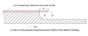
- When the electroplating of the board is finished trace is etched through the use of a trace etching machine. The thickness of the trace causes vertical etching when horizontal etching is done. So to compensate the side etching trace required to be compensated. The side etching can be seen
Industrial standard for Trace width compensation
- The value of compensation for one ounce of copper thickness is given here

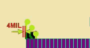
- There are some problems caused by the compensation such as if spacing among the original line and copper foil is four mil trace required to be compensated at one side through 0.3 mils and left side copper foil also needs to be compensated by 0.3 mils. So real spacing after compensation will be 4mil-0.3mil-0.3mil=3.4mil. Through 3.4 mils is less than production process features that is for the regular board at PCBWAY is six mil
- For this point, engineers will eliminate the left side copper foil since they know that eliminating the left side copper foil will not affect the trace and it is significant to make sure the structure of the independent trace on the right side. In the result file given by the users will be modified
Drill Compensation
Causes for Drill compensation
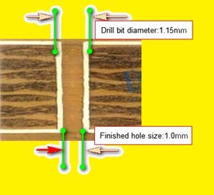
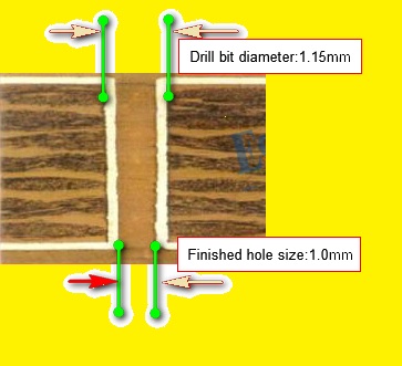
- The hole size given in Gerber files that is provided by the customers normally defines the finished hole size. During PCB manufacturing, copper plating is applied in the hole which results in a reduction of hole size. To make sure that the finished hole size is according to demands drill compensation is performed to make an accurate hole size
- For instance, if customers need a final finished hole size of 1.00 mm with immersion gold, IPC standard class II and 0.25mm compensation for hole size engineers of PCBWAY will choose a 1.15mm drill bit for hole drilling
industrial Standard for Drill Compensation
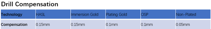
- The compensation value relies on the compensation parameters designed on the basis of industry manufacturing ability testing results. The drilling compensation parameters in the complete industry are the same.
Pad Compensation
- During the desing of the pad on the PCB surface errors taken into account in construction, size, and structure must be settled according to components requirements and get good connections and reliable electrical operation.
- Pad compensation is a sign to point in PCB construction resulting in enhanced quality and reliability of soldering. Factors such as temperature pressure and material during PCB construction real size and shape of pads can be different from the desing. If compensation is not done it can result in loose connections, bad soldering, and in some cases soldering failure
- Commonly used techniques for pad compensation are listed here
Diameter compensation
- Dia adjustment of the solder pad to match the component normally increases of decreases diameter by about ten percent according to real conditions.
Shape compensation
- Shape adjustment of solder pad changes from circular pad to square or elliptical pad or addition of protrusion or indentations to the edge of the pad to modify its shape
Spacing compensation:
- The adjustment of the distance between neighboring pads is normally not less than 1.2 times the width of the pins’ components. During pad compensation, it is significant to take into consideration the soldering process, component pin spacing, and PCB design to ensure reliable connection and high-quality soldering
- There are some problems caused by the pad compensation are shown here
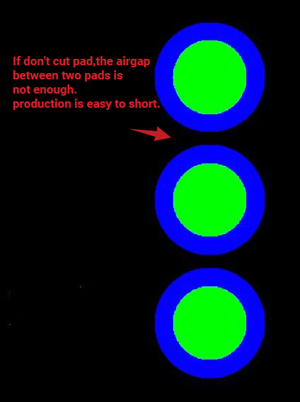
- According to PCBWAY manufacturing abilities, it is suggested that spacing between pads for BGA and IC must not be less than 0.15mm. If the spacing is less than 0.15mm solder pad compensation will be done to minimize short circuitry and fulfill production demands
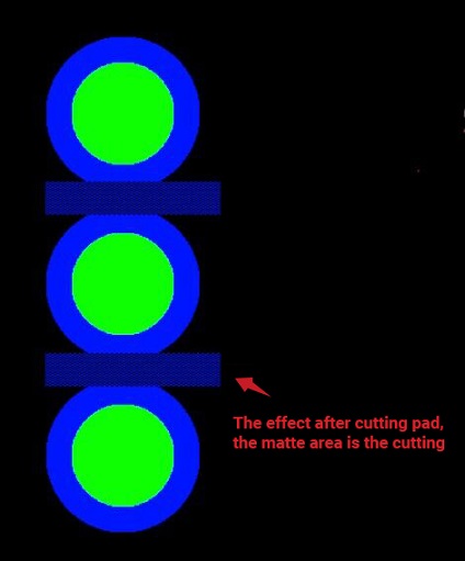
- Cutting effects are shown here
Material Compensation
- Material compensation in the manufacturing process of the board is a significant phase aimed at compensating for material expansion, contraction, and some other problems that can arise during board construction. It is performed to make sure that the dimensions and shape of the board are stable throughout the manufacturing process
- Material compensation is required according to the below-mentioned parameters
The thermal expansion coefficient of materials:
- Different material has differnt thermal expansion coefficients that will affect the size and shape of the board. So in the production process of the board, it is compulsory to compensate the size of the board on the thermal expansion coefficient of the required material, to make sure the size and shape of the board help the continuous production.
selection of size and material of the printed circuit diagram:
- The size and material of the PCB diagram also affect the size and shape of the board. So in the production process of the board, it is compulsory to consider the size and material used fo the printed circuit diagram and create fine compensation based on actual demands
Control of manufacturing process parameters:
- In the production process of the board it is compulsory to control manufacturing process features like temperature humidity heating etc that help to ensure the size and structure of the board remain stable throughout the manufacturing process. With that, it is also compulsory to adjust different construction processes to fulfill the construction needs of different types of PCB boards
Electrical Characteristic Compensation
- The electrical parameters of the baord like impedance and capacitance can be affected through the routing of trace, board material, and vias. So finest compensation measures are required to ensure sure operation of the board
- Electrical characteristic Compensation consists of the following aspects:
Resistance compensation:
- Resistance is the basic electrical parameter of PCB board circuits. For board, desing and construction resistance value can be affected by numerous factors like substrate material, trace width,, and trace spacing wiring technique. To ensure sure operation of the circuitry good compensation measures are required for resistance
Capacitance compensation:
- Capacitance is also an important parameter in PCB designs. During the designing and manufacturing of the baord capacitance value can be affected by many factors like trace width, trace spacing length of trace, and wiring technique. To make sure operation circuitry fine compensation is needed
Signal delay compensation
- Signal delay refers to the time it takes for a signal to travel in a PCB circuit. In the PCB design and manufacturing process, the signal delay value can be affected by various factors, such as substrate materials, trace width, trace pitch, trace length, wiring method, etc. To ensure signal timing performance, appropriate compensation must be made for delay measures signal.
Impedance matching compensation
- Impedance matching refers to matching the output impedance of the signal source to the input impedance of the load to achieve the best signal transfer effect. In the design and manufacturing process of printed circuit boards, the impedance matching value can be affected by various factors such as trace width, trace spacing, connection method, etc. Appropriate compensating measures must be taken to ensure impedance matching of the signal. gate for impedance.


