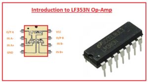
Hello, readers welcome to the new post. Here we will discuss Introduction to LF353N Op-Amp. The LM353N is designed as an input amplifier for low-noise, low-current, and fast-switching audio applications commonly used in dual-supply operation. It features a highly stable, programmable output stage, low noise, and is based on the latest CMOS technology. So let’s get started with Introduction to LF353N Op-Amp.
Introduction to LF353N Op-Amp
LF353 device is a low-cost and high-speed JFET input operational amplifier that comes with a low input offset voltage value.
it needed a low supply current to maintain a larger gain bandwidth and high-speed slew rate.
With that matched high voltage JFET input has low-value input bias and offset current
LF353 can used for projects where high-speed integrators, digital to analog converters, and some other projects.
Its operation temperature is about 0°C to 70°C.
It is designed by Texa instruments.

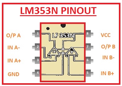
Pinout
Features of LM353N
- It comes in PDIP packaging
- Its input has a high value of impedance
- Gain bandwidth is four megahertz
- Input volts are ±18 volts
- It has eight pinouts
- Low Input Bias Current 50 pA
- Low Input Noise Current 0.01 pA/√Hz
- Low Supply Current 3.6 mA
- High Input Impedance 1012 Ω
- Internally-Trimmed Offset Voltage
- Gain Bandwidth 3 MHz
- High Slew Rate 13 V/µs
LF353N Applications
- It is used for low-noise audio circuits and high-input-impedance designs
- it is part of the sample and holds the circuit
- it is also used for high-speed Integrator
Electrical Specifications:
- Input offset voltage is 5mV to 10mV.
- Input offset voltage drift = 0°C≤T≤+70°C) is 10µV/ °C.
- Input offset current is 25 to 100pA and 4nA
- The input voltage range is ±11V to ±15/-12V.
- CMRR is 70-100dB.
- The power supply rejection ratio ( is 70-100dB.
- Input bias current 50-200nA and 8nA
- Input resistance is 10¹²Ohms.
- Maximum signal voltage gain value is 25-100V/mV
- Output voltage swing is ±12V to ±13.5V.
- slew rate is 13V/µS.
LF353N vs. LF353P
- LF353N is a dual operational amplifier that comes with inner compensated input offset voltage.
- LF353P is a high-speed JFET input operational amplifier that has low input offset voltage. it needed low supply for maintaining a larger gain bandwidth fast slew rate.
F353N vs KA4558 vs LM258N Comparison
| Part Number | KA4558 | LF353N | LM258N |
| Manufacturer: | ON Semiconductor | ON Semiconductor | ON Semiconductor |
| Description: | IC OPAMP GP 2 CIRCUIT 8DIP | IC OPAMP JFET 2 CIRCUIT 8DIP | Operational Amplifiers – Op Amps Dual OP amp |
| Lifecycle Status: | LIFETIME | – | LAST SHIPMENTS |
| Mount: | Through Hole | Through Hole | Through Hole |
| Mounting Type: | Through Hole | Through Hole | Through Hole |
| Package / Case: | 8-DIP (0.300, 7.62mm) | 8-DIP (0.300, 7.62mm) | 8-DIP (0.300, 7.62mm) |
| Number of Pins: | 8 | 8 | 8 |
| Weight: | 851mg | 851mg | 851mg |
| Number of Elements: | 2 | – | 2 |
| Operating Temperature: | 0°C to 70°C | 0°C to 70°C | -25°C to 85°C |
| Packaging: | Tube | Tube | Tube |
| Published: | 2001 | – | 2011 |
| JESD-609 Code: | e3 | e3 | e3 |
| Pbfree Code: | yes | no | yes |
| Part Status: | Last Time Buy | Last Time Buy | Obsolete |
How does a voltage follower work?
- Voltage follower generated output signal that is same with amplitude with input signal. Since the input signal is provided to the non-inverting input terminal, and there is no inversion occurs. So voltage follower is the noninverting buffer.
What is the minimum supply for LM358?
| Compliance (Only Automotive supports PPAP) | Standard |
|---|---|
| Minimum Supply Voltage (V) | 3 V |
| Maximum Supply Voltage (V) | 32 V |
| Supply Current 5V (per Op Amp) (mA) | 0.5 mA |
| Input Offset Voltage typ (mV) | 2 mV |
Is op-amp output AC or DC?
- The operational amplifier is a high-gain voltage amplifier. It is used for amplification of signals through increasing magnitude. Operational amplifiers can amplify DC and AC signals.
Can LM358 be used as a comparator?
- LM358 comparator IC comes with 2 operational amplifiers that show two comparators in one IC. For using LM358 as a comparator there is a need to connect the power supply with the Vcc and GND pin of LM358 IC to activate IC
What is the difference between LF353N and LF353P?
- LF353N is a dual amplifier having compensated input offset voltage. The LF353P is a high-speed JFET input operational amplifier having low input offset voltage. it needed a low supply current for maintaining a larger gain gain-bandwidth product and a fast slew rate.
What is the difference between LF353N and LF356?
- The working of these two amplifiers is almost the same and both are part of CMOS input Op. LF356 comes with a low slew rate high bandwidth and small offset current. IF it is used normally it can be replaced. Focus on dual op-amp and single op-amp.
What is the working principle of IR transmitter circuit?
- The emitter is an IRD LED and the detector is an IR photodiode. The IR photodiode is sensitive to IR light emitted through IR LED. The photodiode resistance and output voltage vary in proportion to IR light obtained. That is the working principle of the IR sensor.
Read also


