Hello dear FSC students, I hope you all are doing great. In today’s tutorial, we will have a look at 2nd Year Physics Chapter 18 Solved Questions. I have started a series of tutorials related to the solution of questions given in 2nd-year physics. In the previous tutorial, I have discussed all the questions of chapter17 with the detailed.
In this post, we will have a detailed look at all the questions given in chapter 18 of FSC physics. I will explain all the questions one by one and give an answer to every question in a simple way. So let’s get started with 2nd Year Physics Chapter 18 Exercise Solved Questions.
2nd Year Physics Chapter 18 Exercise Solved Questions
Question 18.1
- The majority charge carrier in N-type materials are free electrons and holes are majority charge carriers in P-type substance.
- The electrons move from less potential to high potential while holes move from high to low potential.
- The movement of electrons in N material is faster than the motion of holes in P-type materials.
Question 18.2
- Both N and P-type materials are electrically neutral. Because these substances are constructed with a mixture of pure atoms of semiconductor and impurity atoms both are neutral.
Question 18.3
- The anode of (P-type material) has a high potential value of 0.2 volts then the cathode (N material).
- So ‘P’ Part of the diode is positive than the N side of the diode. It means that the PN junction is in forward biasing condition.
Question 18.4
- During the formation of the depletion region, some electrons from the N side of the diode move to the P part and combine with the holes to make neutral them. Due to that flow of current stops due to the creation of potential barriers.
- There are at both sides of PN junction is known as depletion region since all charges carriers electrons and holes have been eliminated through this region.
Question 18.5
- During forward biasing the area of depletion region decreases while in reverse biasing the area of reverse biasing increases.
Question 18.6
- For silicon diode energy gap between valence and condution band is one electron volts.
- When an electron moves from conduction band to valence band it releases photon having an energy of one electron volt.
- The energy value of one electrons volts does not lie in a visible range of electromagnetic radiation.
- So light does not release by the silicon diode.
Question 18.7
- The operation of photodiode based on the detecting of light. It operated in reverse biasing because in reverse biasing condition the current is very less when voltage is provided to the diode.
- When light falls on the depletion region of diode pairs of electrons and holes created due to that current start to flow.
- The quantity of current flow depends on the intensity of light falling on the diode.
Question 18.8
- As the area of base of the transistor is less and there is lightly doped in this region.
- So carriers coming from the emitter of a transistor become neutral in very less amount in base.
- Due to that less base current flows.
- During the reverse biasing conditions of a collector-base junction, all electrons go to the collector part of the transistor.
- Some charge carriers move through the base and less amount of current flows through it.
Question 18.9
- For the normal working of a transistor, there should be emitter to a base junction in forward biasing condition and collector to a base junction in reverse biasing condition.
- In-circuit of common emitter amplifier these conditions can be got by using 2 batteries VBB and VCC.
- For this connect VBB with the emitter-base junction in forward biasing condition and VCC with the collector-base junction in reverse biasing condition.
Question 18.10
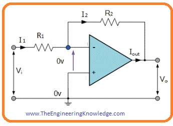
- For the operational amplifier circuit, AOL is an open-loop gain whose value is 105.
- So for given Vo
(V+ -V-) = 0
V+ = V-
- If V+ connected with the ground terminal then V- becomes ‘0’ which is (V- = 0).
- So inverting input will be grounded.
- From the below figure.
V- -Vi) /R1 = (V- –Vo)/ R2
(0-Vi )/R1 = (0- Vo)/R2
Vo/Vi = -R2 / R1
G = – R2 /R1
Question 18.11
(a):
- As input is 1 and 0, the output is zero it means gates can be And, XNOR, NOR gate.
(b):
- Inputs are 1 and 0, the output is 1 so gates can be OR, NAND, XOR Gates.
Related Posts
- 2nd Year Physics Chapter 12 Exercise Solved Questions
- 2nd Year Physics Chapter 13 Exercise Solved Questions
- 2nd Year Physics Chapter 14 Exercise Solved Questions
- 2nd Year Physics Chapter 15 Exercise Solved Questions
- 2nd Year Physics Chapter 16 Exercise Solved Questions
- 2nd Year Physics Chapter 17 Exercise Solved Questions
- 2nd Year Physics Chapter 18 Exercise Solved Questions
- 2nd Year Physics Chapter 19 Exercise Solved Questions
- 2nd Year Physics Chapter 20 Exercise Solved Questions
- 2nd Year Physics Chapter 21 Exercise Solved Questions
So friends it the detailed post about 2nd Year Physics Chapter 18 Exercise Solved Questions if you have any questions about this post ask in comments. See you in the next post about solution of chapter 19 exercise. Have a good day. Thanks for reading.


My brother suggested I might like this web site. He was totally right.
This post actually made my day. You can not imagine simply how much time I had spent for
this information! Thanks!