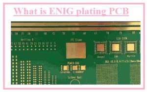
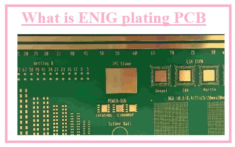
 Hello, guys welcome to the new post. Here we will cover What is ENIG plating PCB. Full form of ENIG is electroless nickel immersion gold plating that is performed on PCB boards that have a larger number of coppers pads. The component of projects connected to the PCB board gets the current from the board. In ENIG there are 2 layers of the metal coating is done. At the ist layer of copper pads that exist on the PCB board, the Nickle layer is coated after that thin layer of gold plated.
This type of plating is performed at the upper layer of the copper pad since this plating offers conductive behavior in a good way. That also helps to give fine protection from oxidation and other environmental conditions. Either it is expensive but used due to fulfilling the RoHS criteria. Numerous PCB suppliers also fulfill the RoHS in their services such as PCBWAY. That is best in all services also offering ENIG plating services with reasonable prices and good quality since they are equipped with professional engineers and machines. For more than ten years they have been fulfilling the prototype and fabrication demands of their customers with high-quality boards, fast delivery, and less expensive products. Since it is the best and most featured PCB manufacturer in China it prides itself to be your best business partners as well as a good friend in every aspect of your PCB needs.
PCB is one of the most important components of any electrical and electronic equipment. PCB quality determines the quality of all these devices. Modern technology makes it possible to increase the miniaturization of composite circuits, higher packaging density, and smaller building sizes, which is why higher demands on PCBs arise.

Introduction to ENIG plating PCB
- The most commonly used PCB plating is ENIG. At the bare PCB board, the coating application is called PCB surface finishing.
- The use of ENIG and other types of coating such as HASLis to save the board from external harsh conditions such as corrosion
- ENIG is plated on the pads of coppers existing on the board surface which helps to fight external conditions not favorable for the board.
- First of all copper layers are plated with nickel then the gold layer. The use of ENIG helps to board get an easy soldering process and avoid resistance and plane surface.
- Due to the complicated nature and high cost also been used since fulfilling the RoHS.
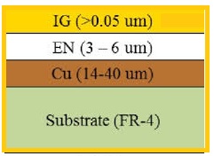
- ENIG consists of two metal layers first is Nickle on the copper that helps to connect the components.
- Another is a gold layer that reduces the connection with other parts. The value of the Nickle layer is four to seven micrometers and gold thickness lies 0.05 to 0.23 micrometers.
- The temperature needed for ENIG is eighty centigrade
Advantages of ENIG Plating PCB
- Some main advantages of ENIG plating are discussed here
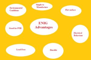
Simple to Manufacture
- Its creation process is simple and easy. Numerous PCB board designers used this plating process for the creation of boards.
Flat surface
- This plating comprises two layers having a metal coating of nickel that protects the surface and easy to connect components.
- This plating fulfills the needs of flat surfaces like BGAs.
Resist to Environmental Conditions
- Every PCB manufacturer prefers to use such a board that resists to oxidation this plating gives this feature. But other surface finishing lack this feature.
- For protection from the oxidation gold layers with nickel is employed on the board.
Fine Electrical Behaviour
- This plating also offered a better electrical operation to board than other plating techniques these parameters also covered with others such as the connection of wires, and finishing design.
A large value of temperature resistance
- The board used in instruments used in medical and military purpose bear the larger value of temperature conditions.
- ENIG finish board comes with these features to handle high-temperature conditions.
Durable
- The finishing used on the board defines the operating life of the board. ENIG plating helps the board to work for twelve months or more. So it is preferred for different project creations.
Lead-Free
- The use of lead inboard can be harmful to health and cause different diseases such as kidney, heart, etc.
- But ENIG plating comes with lead-free features and reduces the cause of harmful diseases due to the board.
Good for PTH
- It is considered as best finishing for PTH. That has wires coming out from the different parts of a breadboard.
Disadvantages of ENIG Plating
- With the same benefits of this plating also have some disadvantages that are described here
Expensive
- It is considered s fine option for different boards but it is an expensive technique. Some customers used other plating techniques due to larger costs but also used in different projects.
Repairing is difficult
- As this plating is done through the use of machines so engineers face difficulty making again the board if damaged.
- In some case, damage is such that cannot be repaired again and users have to get a new board.
Complex Manufacturing
- Its other drawback is that its manufacturing process is difficult. Other types of plating offered a less complex process than he ENIG.
- Since it was created with the use of machines if machines are not configured accurately then cause serious problems during construction
What is the difference between ENIG and electroplating?
- ENIG’s full form is Electroless Nickel Immersion Gold commonly called Immersion Gold. Contrary to gold plating, ENIG is processed through a chemical reaction and does not use electroplating. First copper is covered through a thin layer of nickel and then a thin layer of gold is applied.
What is the difference between PCB surface finish HASL and ENIG?
- HASL is more hazardous than ENIG. The selection of ENIG then HASL, reduces the use of lead and releases from flux and fusing oil. HASL is lower cost than ENIG for 2-layer boards but can used for more layers, prices of ENIG and HASL plating are almost close to each other.
That is all about the ENIG plating PCB. all details has been discussing the ENIG plating PCB. If you have any further query ask inc comments. thanks for reading have a good day.


