Thin film technology is a new technique used for the creation of PCB boards that come with different features and high-performance operation as compared to rigid or thick film circuits. Currently used different devices and projects like mobile phones, and smartwatches, are made with flexible circuits due to reshaping in different structures. With the use of ultra-thin coatings on thin film boards we can make high-density circuits easily in smaller packages.

Thin-Film Circuit Boards Overview
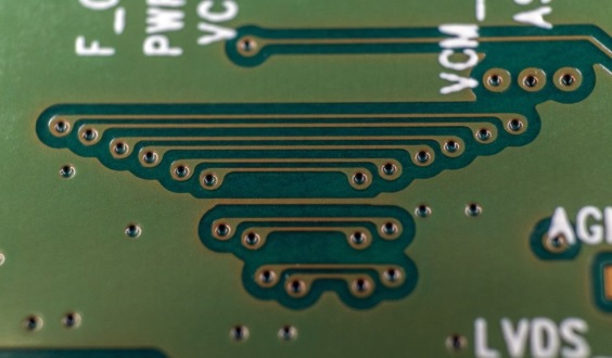
Thin film circuit boards also called flexible PCB boards come with component configurations in different layers of conductive and insulating materials. Conductive layers are in pattern form for making the connections of components of circuits.
Flexible boards come with some components of rigid boards and have design features that can move small packaging. There is a flexible substrate used for this technology as compared to a rigid substrate.
Normally conductive materials used aer aluminum, silver ink, or carbon. Materials used for the substrate are quartz, glass, ceramic, and organic materials. Non-conductive substrate materials used are polyimides, PET (polyethylene terephthalate), FR-4, and PEEK (polyether ether ketone).
Flexible boards come with single copper layers but have higher functions than more layers. Multilayer boards make connections through the use of through through-holes process.
Some boards come with rigid-flex boards combination that comes with flexible and inflexible circuit combinations to make the hybrid structure.
Metallic or copper layer thickness for boards is about 0.5 oz to 13 oz, insulating layers is 0.17 mm and 7.0 mm thick.
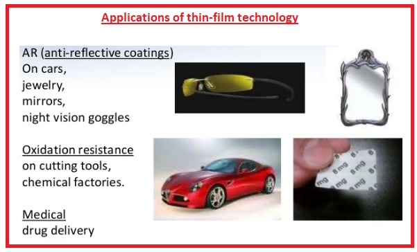
Thin Film Circuit Applications
- Thin film boards are used for high-frequency applications like microwave devices, communications systems, and radar systems since they come with low signal losses and high-frequency features
- They are also part of the aviation industry and military instruments that need miniaturization and high performance such as navigation systems, and military-grade electronics.
- This board is also part of the telecom sector where high-speed data transmitted and signal quality is important like in data centers.
- It is also used to make medical devices such as sensors, and high-frequency components and provide them reliability and compactness. It is part of medical imaging devices or diagnostic equipment.
- These boards are also used for LED, photodetectors, and fiber optics since are compatible to optical materials and accurate manufacturing requirements fulfilled through these boards
- it is also used in audio instruments or high-speed data-processing components
Laser Patterning for Thin-Film Circuits
Conductive coatings for PCB boards help to current flow in different components through the use of substrates like quarts of glass, polymers, or silicon. The laser pattern manufacturing techniques remove components of conductive layers for making circuits.
laser patterning offers more flexibility for different projects and reduces the use of materials for board creation as compared to the photolithography process. The control of disruption is difficult for layer patterning but the use of front and back processing can reduce the errors
Faqs
- Semiconductor thing filme come with semiconductor material layers that are applied in some nanometer to microns range in thickness on the substrate through the use of different deposition methods like chemical vapor deposition (CVD) or electron beam (e-beam) evaporation


