Hi, readers welcome to the learning place. In today’s we will have a detailed look at Introduction to Summing Amplifiers. A summing amplifier is a type of amplifier circuits that added to inputs given at the inputs terminals and provides one single result. At the input side, the different signal is provided in parallel combination. The two main types of circuits are used in this module first one is the inverting and second one is non-inverting.
To get output from this circuit ohm law is applied. The input signals are delivered to the input terminals through the use of resistance in the path of the signal. The parameters of the input signal are in directly proportional to the connected resistance. In today’s post, we will have a detailed look at its working, operation circuit configuration, and some other related factors. So let’s get started with Introduction to Summing Amplifiers.
Introduction to Summing Amplifiers
Summing Amplifier with Unity Gain
- The summing amplifier is the category of an amplifier circuit that has 2 or larger than 2 input terminals and one output terminal. The value of output signal is equal to the negative of the addition of 2 inputs signals.
- In below figure the circuit of summing amplifier having 2 inputs is shown.
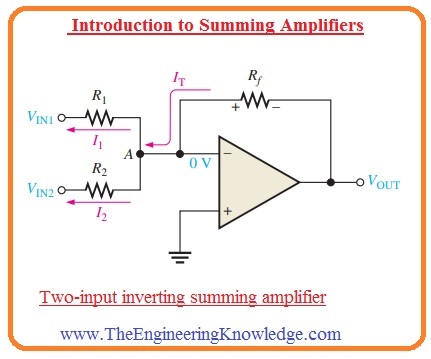
- The working of this circuit arrangements and related output results are discussed here.
- The 2 input voltage signals VIN1 and VIN2 are provided at the input and generate 2 current I1 and I2 as you can see in the figure.
- If we take into consideration the infinite input impedance and the virtual ground we will find that the value of the inverting input terminal of the operational amplifier has zero volts and there is zero current is passing through it.
- It indicates that the net current IT that is passing in the resistance Rf will distribute in the 2 current I1 and I2 at a point denoted as A in the circuit that is summing point.
(IT = I1 + I2)
As the VOUT = -ITRf
VOUT = -(I1 + I2)Rf
=-[(VIN1/R1)+(VIN2/R2)]Rf
- Let’s assume that the value of resistance R1, R2 and Rf are similar to R then we have.
VOUT=-(VIN1/R+VIN2/R)R
-(VIN1 + VIN2)
- This equation shows that the output signal is equal to the addition of 2 inputs signal with reverse polarity.
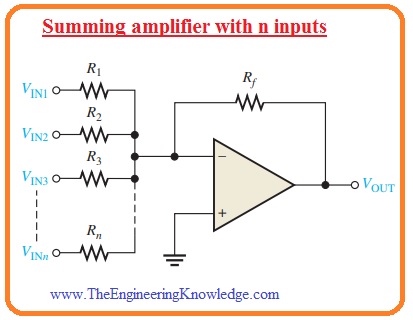
- The equation for unity gain summing amplifier having n number of input is mention here and circuit also shown below.
VOUT =-(VIN1 +VIN2 a+VIN3 +…….+VINn)
Summing Amplifier with Gain Greater Than Unity
- If the value of resistance Rf is greater than the input resistance the value of amplifier gain is Rf/R in this case the R is equal to the every input resistance.
- The value of the signal at the output will be given as.
VOUT =-Rf/R (VIN1+VIN2 Á+…+ VINn)
- We can observe that the value of the output signal is equal to the addition of complete input signals having multiple with the constant -(Rf /R).
What is Averaging Amplifier
- This amplifier circuit is created to generate the mathematically average of the signal given at the input terminal.
- It can be created by making Rf/R equal to the inverse of n inputs.
Rf/R = 1/n
What is Scaling Adder
- The different values can be given to every input of the summing amplifier circuit through varying the value of resistance at the input. We can see that the output signal can be mentioned as.
VOUT=-[Rf/(VIN1)+ Rf/R2(VIN2)+…Rf/Rn(VINn)]
- The value of certain input is regulated through the ratio between resistance Rf and Rx for a given value of input resistance (Rx. R1, R2, … Rn).
Applications of Summing Amplifier
- The digital to analog transformation is a very significant technique used for the transformation of the digital signal in the analog signal.
- The example of this is a sound signal that is transformed in the digit form for storing purpose, processing and sending from one point to another and after reaching at receiving end int converted in the original sound.
- The one technique for digital to analog transformation is use of scaling adder having input resistance which denoted the binary value of the input in form of digital.
- It is not the most generally used technique it uses to describe the usage of scaling adder.
- Instead of this technique the most commonly used technique for digital to analog transformation is R/2R ladder technique.
- We will discuss the R/2R ladder is used for comparison purposes.
- The below figure indicates the 4 digit DAC of R/2R category.
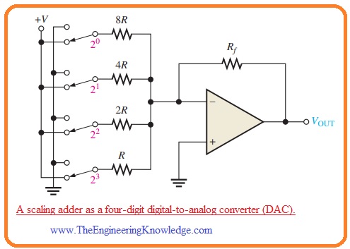
- The symbolic representation of switch is denoted the transistor switches using for every 4 binary number applied at input terminals.
- The inverting terminal is connected at virtual ground and therefore output signal is in direct relation to the current passing in the feedback resistance Rf.
- The least value of resistance R related to the largest binary input value 23
- As it is above mentioned that the R/2R ladder is the most commonly used digital to analog converter circuit than the scaling adder and it is shown in below figure.
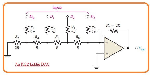
- The benefit of this circuit is that it uses only 2 resistances.
- Let us suppose that D3 input has a high value or five volts and the other is connected with the ground. This state indicates binary no is one thousand.
- The circuit analysis indicates that it will decrease the resultant circuit to shown in figure denoted as a.

- It is compulsory that there is no current is passing through the resistance 2R since the inverting input is linked with the ground.
- So all of the current passing in the resistance R7 is also passing in the resistance Rf and the value of output voltage is minus five volts.
- The operational amplifier retains the inverting input close to the 0 volts due to negative feedback configuration.
- So-net current is passing in the resistance Rf than in the inverting input.
- The figure denoted as b indicates that resultant circuitry for the input D2 at a voltage value of five volts and the other are linked with the ground.
- This state indicates the condition of 0100.
- If we use the Thevenin theorem at resistance R8 we will have 2.5 volts in series combination with the resistance R.
- Due to it current passing through th resistance Rf that gives the voltage value of -2.5 V.
- The circuit denoted in figure C indicates the resultant circuitry for D1 input is connected at five volts and all others are linked with the ground terminal.
- This situation denotes the condition of 0010.
- If we again apply Thevenin theorem at resistance R8 we will get 1.25 volts in series combination with the resistance R.
- It causes the current in the resistance Rf that provides an output voltage of -1.25 V.
- In figure circuit denoted as d’ represents the situation when the D0 has five volts across it and other inputs are linked with the ground. It defines the condition of 0001.
- If we apply Thevenin theorem at resistance R8 it provides 0.625 volts in series combination with the resistance R. The current passing through the resistance Rf provides value of -0.625 volts at the output.
Read also
- LM324 – Single Supply Quad Operational Amplifiers worksheet
- Difference Between An Operational Amplifier and Comparator
- Audio Amplifier Circuit
- What is LM709 Operational Amplifier?
So friends that is detailed post about Introduction to Summing Amplifiers if you have any further query ask in comment. Thanks for reading have a good day.