Hi friends welcome to the new post. Here we will learn ATMega328p Pinout Configuration, Features & Datasheet. Microcontrollers are the main component of electronic and automation circuits. The controller Atmega328P is important due to its flexible operation and is normally used in different embedded system applications. Here we will discuss its working, features, and other parameters. So let’s get started with ATMega328p Pinout Configuration.
Introuctiont to ATMega328p
- The ATmega328P is a low-power, CMOS eight-bit microcontroller that comes with RISC architecture. With the application of different commands in a single clock cycle, it helps to get one million instructions per second in megahertz.
- It helps to optimize the power used with processing speed. This board was made by Atmel now it belongs to Microchip technology.
- It is normally used due to used as the main control in different Arduini boards for example Arduino Pro Mini, Arduino UNO, etc.
- it has about 131 instructions mostly used in on clock cycle. From 16 MHz clock frequency, we can get about 16 MIPS throughput
Atmega328P PINout Configuration
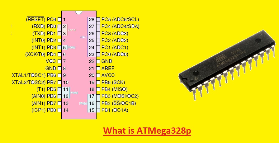
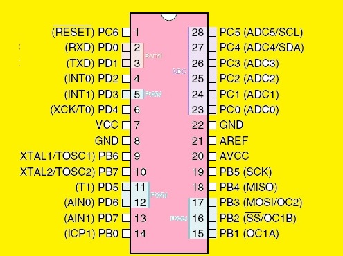
There are different comes with 28 pinouts each with has certain function and all are explained here
| Serial no | Pin name | Details | Function |
| 1 | PC6 | PORTC PIn no 6 | it is used as a reset pinout. For programming of RSTDIBL fuse this pin is used for input and output |
| 2 | PD0 | PORTD pin Pin0 | it is used for providing the input data to USART and also used for programming |
| 3 | PD1 | PORTD Pin1 | it is the output pin for USART also used for programming with used for External Interrupt 2 Input |
| 4 | PD2 | PORTD Pin2 | it is an External Interrupt source 0 pinout
|
| 5 | PD3 | PORTD pin no 3 | It is External Interrupt source pin1 and OC2B |
| 6 | PD4 | PORT D Pin4 | it used as a Timer0 External Counter Input and USART External Clock I/O |
| 7 | VCC | it is attached with a positive voltage | |
| 8 | GND | ground connection | |
| 9 | PB6 | PORT B pin 6 | Chip Clock Oscillator pin 1 and TOSC1 |
| 10 | PB7 | PORT B Pin7 | it is XTAL2 (Chip Clock Oscillator pin 2) and TOSC2 (Timer Oscillator pin 2) |
| 11 | PD5
| PORT D Pin5 | it is Timer1 External Counter Input and OC0B(PWM – Timer/Counter0 Output Compare Match B Output) |
| 12 | PD6 | PORT D Pin6 | it is AIN0(Analog Comparator Positive I/P) and OC0A(PWM – Timer/Counter0 Output Compare Match A Output) |
| 13 | PD7 | PORTD Pin7 | it is an Analog Comparator Negative I/P
|
| 14 | PB0 | PPORT B pin 0 | it is Timer/Counter1 Input Capture Pin) and CLKO (Divided System Clock. |
| 15 | PB1 | PORTB Pin1 | it is Timer/Counter1 Output Compare Match A Output |
| 16 | PB2 | PORTB Pin2 | it is the Slave Select Input pin, it’s low when the controller acts as a slave. |
| 17 | PB3 | PORTB Pin3 | Master Output Slave Input, controller works as slave data get this pin |
| 18 | PB4 | PORTB Pin4 | it is also Master Input Slave Output |
| 19 | PB5 | PORTB Pin5 | It is an SPI Bus Serial Clock and clock shared between this controller and another system for accurate data transfer. |
| 20 | AVCC | Power for Inner ADC Converter | |
| 21 | AREF | Analog Reference Pin for ADC | |
| 22 | GND | Ground connection made | |
| 23 | PC0 | PORTC Pin0 | ADC Input Channel 0 |
| 24 | PC1 | PORTC Pin1 | ADC Input Channel 1 |
| 25 | PC2 | PORTC Pin2 | ADC Input Channel 2 |
| 26 | PC3 | PORTC Pin3 | ADC Input Channel 3 |
| 27 | PC4 | PORTC Pin4 | ADC Input Channel 4 and Two-wire Serial Bus Data Input/Output Line |
| 28 | PC5 | PORTC Pin5 | ADC Input Channel 5 and SCL |
ATMEGA328P Features
- It has an eight-bit AVR CPU
- 28oins configured on this module.
- its operating voltage is +1.8 V TO +5.5V.
- it has 23 programmable I/O lines
- (17,18,19 PINS) are used as Master/Slave SPI Serial Interface, (2,3 PINS) used as Programmable Serial USART, and (27,28 PINS) Two-wire Serial Interface.
- it does not have a JTAG Interface
- it has 6channels and 10-bit resolution ADC
- 12,13 PINS used as analog comparator
- 6 PWm configured on it
- it has 32Kbytes[10000 write/erase cycles] flash memory
- its CPU speed is 1MIPS for 1MHz
- Comes with 2Kbytes Internal SRAM
- it comes with a Programmable Watchdog Timer with a Separate On-chipOscillator
- its working temperature is -40°C to +105°C.
ATmega328P IC Packages
The ATmega328P is available in 4 IC Packages. that are listed here
| Package | Pinout |
|---|---|
| 32-Lead TQFP | Slightly different |
| 28-Pin SPDIP | Slightly different |
| 32-Pad VQFN | Slightly different |
| 28-Pad VQFN (MLF) | NaN |
How to Use Atmega328P
- The uses of ATmega328P are like other controllers. Before it gets programmed. There are many software used to program this module.
- Commonly used controllers are Arduino board and Arduino software that is Arduino IDE used to program this controller.
- IDP programmer is also used for programming created for AVR controller called Atmel studio that can be downloaded free from Atmel codes in IDE or IDP programmer.
How to Safely Run Atmega328P
- For the long-term operation of this model in different electronic projects, you must use it carefully since it is sensitive. Its input voltage must not be more than 5.5 volts. Check the voltage source output before making a connection.
- During connection on a breadboard or permanent connection in the circuit it is suggested to check the pinout for a short circuit before connecting power, best to use an IC socket for the integrated circuit and must check IC socket pinouts for short circuits before connection IC.
- IC socket also saves IC from getting heat from the soldering iron in the soldering process. Try to operate this module above the -40 centigrade and above 105 centigrade.
Atmega328P Bootloader
The Atmega328P microcontroller’s bootloader software is embedded in a permanent memory unit that works as the initial stage for implementing additional software. its main work is to ready the controller for working, and make it easy to upload external programming devices without the use of code. During the reset state of Atmega328) this bootloader checks the existence of connected software. This integration program is easy to use and offered by Arduino, which uses Atmega328P widely.
Where to Use ATMEGA328P
it is famous for its cost and easy-to-use featues. ARDDUINobaords are made on this module since it has different features explained here
- it has 32 Kbytes program memory, making it useful in different projects.
- It has different power-saving modes so used on MOBILE EMBEDDED SYSTEMS.
- Its Watchdog timer reset error so used with less chance of human interference
- With the latest RISC architectures controllers apply programs fastly
- it has a temperature sensor so easily used in extreme temperatures.
ATMEGA328P Applications
- it used in the digital processing of data
- Configured with different Arduino boards like ARDUINO UNO, ARDUINO NANO, and ARDUINO MICRO boards.
- It used for power regulation system
- Used for digital data processing
- Used in display units
- It is part of the peripheral interface system
- It used in motor control circuits
- Different machines operated on embedded systems like vending machine
Read ALso:
- Introduction to Arduino Mega 2560 Rev3
- HOW TO DO MATH OPERATION in ARDUINO
- Introduction to 1n4148 Datasheet
Faqs
How many pins does ATmega328P have?
ATmega328/328P comes with 28 pinout
What is the function of ATmega328?
ATmega328 is used in different projects and systems where low-powered and low-cost controllers are needed.
What IC is ATmega328P?
it is an 8-bit microcontroller based on AVR RISC architecture
Why is ATmega328P used?
It’s low power and low-cost structure make it effective to use
What is ATmega328P theory?
It is an advanced virtual RISC controller. Supported eight-bit data processing. It comes with 32KB inner flash memory and 1KB EEPROM.
Why is it called ATmega328P?
It is a low-power CMOS 8-bit microcontroller based on the AVR enhanced RISC architecture.
Is ATmega328P a processor?
ATmega328 is a single-chip microcontroller made by Atmel in the megaAVR family
What is the meaning of ATmega?
Atmega is a microcontroller, under the AVR group by Atmel
What is P in ATMEGA328P?
P in ATMEGA328P is pico power
What is the voltage of ATMEGA328P?
It is operated by 1.8-5.5 volts.
What is the advantage of ATmega328?
Process is easy to use with the 8bit and 16bit then complicated 32/64bit. It can easily used without any extra component with 32k bytes of onboard self-programmable flash program memory.


