SONY DSC
Hello, readers welcome to the new post. In this post, we will have a detailed look at What is PCB Trace. PCB is the basic and most important part of any project that we are constructing and making for our personal and industrial use. Currently, it almost every device-related to electronics uses this board and the structure of this device is manufactured on the board.
At PCB design of the circuit is employed through different components and a copper layer is placed at making a connection of the components. The components are linked through the uses of copper layers traces that are placed at their desired symbol and link with each other to flow current and circuit completion. In this post, we cover basics details about these traces and will also learn how we can get services about these traces to make our PCB according to our projects. So let get started with What is PCB Trace
What is PCB Trace
- The copper traces are the most important part of each and every circuitry board. These are not designed on random basics.
- But there is good search and time taking process to draws these traces according to our projects otherwise it can cause serious problem for our design.
- There are numerous elements are configured at the board and for the configuration of each and every component and part, there is certain types of calculations are needed to assemble these components.
- When we make the design of the board there is certain configuration is needed for the thickness of the PCB board
- For this process, there is a need of certain gravity if we do not take into consideration there will be errors occur in the working of the board like it can cause a flash of serious danger for the project.
- With hearting, the PCB can cause damage to components designed at the board.
- The thickness traces for each category of the board like one-sided double-sided and multilayer is varied according to user and type.
How to Find PCB Trace Resistance
- There is a very basic method used to finds the value of resistance for PCB traces that is ohms law that says V=IR.
- There are many techniques used to get the resistance of copper traces according to the design configuration of the project and the standard formula used for this process is mentioned here.
R=þ.(L/T.W).[1+∝.(temp-25)
- In this equation, T W and L denote the ara of traces that we ar going to measure that is length width, and height.
- þ defies the resistivity of the substance used and ∝ defines the temperature coefficient of copper material
PCB Trace Formula
- The formula used to measure the trace width is mentioned here that normally used according to consideration of IPC 2221.
[I=k*ΔT^0.44*A^0.725]
- In this expression, I indicate the current has a constant value
- ΔT denotes the variation in the temperature and A is the cross-sectional area of trace.
- This equation can be further summarized to get the cross-sectional area
Area[mils^2] = (Current[Amps]/(k*(Temp_Rise[deg. C])^ 0.44))^(1/0.725)
- After that take into consideration the thickness of the trace to get the required width through this formula
Width[mils] = Area[mils^2]/(Thickness[oz]*1.378[mils/oz])
- The application range of this formula for the current value of zero to thirty-five-ampere temperature value is ten to one hundred degrees.
- Here I want to further mentioned that the trace drawn at the inner layer of the board has high than the width of the trace assembled at the exterior layer.
- There is an option available for the design of weight according to requests when you are designing your board at any design software.
- If you are making your design according to your own design and use of skills but if you are new to this field and have less knowledge must move to the different manufacture services that offered these features with reasonable prices.
- Here I want to mentioned and referred to you that the most trustable service provider related to the design of PCB traces is JLCPCB that is china based PCB-related company.
- They are working since 2006 and almost all over the world providing services related to PCB and its related products.
- They offer services related to the EDA, PCB boards, SMT assembly, stencil.
- It is the most famous and worldwide accepted supplier. To get the service visits their site and send orders according to your required board configuration.
- I am also has been a user of the services they always offered good and high-quality services related to our project and never disappoint us.
- Their services are not related to just design but also a manufacturer of different types of boards like one layer board double layer etc according to design requirements.
- They also help to make projects related to your required design configuration and module so you must also visit them to get your required services.
- To avail of their service click here
What is PCB trace Width Calculator?
- The trace width has very important in the design of the board and there is a certain type of considerations are taken into account for this process to avoid any damage.
- The trace performs a function to bear the extreme current used by the load when it damage.
- Due to movement of high current heat is generated in the traces path and certain value of current it burns out and damages the board
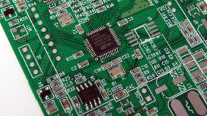
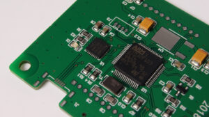
- In the below diagram, we can see the board having traces and component attached
- Traces can also call wiring connections for numerous elements having 0 value of resistances but it not good to say.
- Each trace or path offered a certain value of resistance that creates certain importance for choosing the trace width.
- For proper current carrying value is used to make the width of the trace.
That is a detailed post about PCB traces i tried my level best to make this post simple and easy for you also preferred you best service providers for PCB traces. If you have a further query ask in the comments thanks for reading have a nice day see you in the next post.


