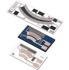
Thick film ceramic PCB board also called thick film resistor ceramic board and this board cooperated with carbon resistor printing on a ceramic substrate with the use of standard PCB methods. Now thick film ceramic board comes with different substrate materials such as high-temperature ceramic to commonly used FR4 board material or also comes in Polyimide (PI) Flex PCB Material.
printed resistor materials come with hydrophobic polyimide resin made to use for polymeric thick film resistors.
On Thick Film Ceramic PCB we can connect different electronic components such as resistor, conductor, and other components after production steps and high-temperature sintering.
Thick Film Ceramic PCB Properties
- Ceramic substrate materials come with 96 percent alumina and the thickness range is 0.25, 0.38, 0.50mm, 0.635mm (default thickness), 0.76mm, 1.0mm.
- Conductive layers materials used are gold palladium, or Mo/Mu+Ni (for Ozone) used
- The conductors used for this board have a thickness >= 10 microns (um), and the Maximum value can be 20 microns (0.02mm).
- Traces width and space for these boards are 0.30mm & 0.30mm, 0.20mm/0.20mm
- It provides tolerance for the final trace is about +/-10%.
- Gold palladium is high cost than silver and about 10~20 times higher.
- Normally used layers for these boards are 1L and 2L that are plated through holes and plated materials are like those used for conductors.
Technical Specifications
- For Typical applications:
- Printing Accuracy= ±2 mil
- Printing Size= 210mm*297mm (Max)
- Line width, Line gape=6/ 6mil (Min)
- Printed only on Ceramic but also on Stainless, FR4, Flexible PCB
- Die assembly and AI wedge bonding
- Resistor value=40mΩ~1000MΩ
- Precision resistor= ±1%,±2%,±5%,±0.5%
- Resistor Accuracy=Absolute ±2%, Ratio ±0.1%
- Laser trim= Functional trim
- Lead out= SIP and DIP, Pitch2.54mm and1.78mm
- Conformal coating and molding
Application of thick film ceramic PCB
- It is used for ignition components.
- It is part of voltage regulator circuits.
- It used for slow motor control circuit
- it used as a thick film resistor for fuel level
- It is used as a blower resistor for a fan motor.
- Mass airflow sensor made on this board.
- it is used for the Throttle position sensor (TPS).
- It is used for rotary position sensors.
- It is used for wiper speed and Automatic leveling system (ALS)
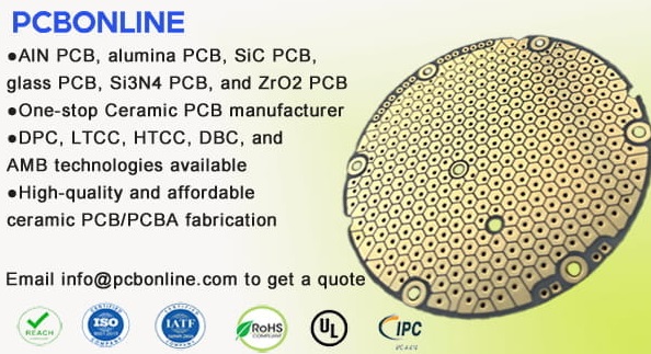
PCBONLINE: High-Quality Ceramic PCB Manufacturer
PCBONLINE is the best manufacturer of ceramic PCB boards and they use 3D DPC methods. With that for ceramic boards, they also use HTCC, LTCC, DBC, and AMB. aluminum nitride PCBs, SiC PCBs, PCB assembly, IGBT modules, COB LED modules, ceramic LED plates, and box-build assembly are all offered by PCBONLINE as ceramic PCBs.
Here are some explanations for using PCBONLINE as your go-to source for ceramic PCB production:
- the thickness of the board made by PCBONLINE is 100nm and 300m.
- They provide high-density and 3-dimensional designs
- Good temperature handling features and welding performance.
- This circuit comes with a longer working life and does not have an oxide layer.
- the dimensions of ceramic PCB are 138 mm by 190mm. The maximum dimension for extreme prototypes is 160mm by 280mm. (Please allow a 4–5 mm space between the edge rails.)
- Available ceramic thickness values are from 0.15 mm to 4.0 mm. (The PCB is 0.1 mm thicker than the ceramic.).
Future of Thick Film Ceramic PCB
Thick Film Ceramic PCB is a new technology that provides the best features for embedded resistors by reducing the use of special termination methods like immersion silver, silver palladium, or gold palladium. With provides high performance and a stable system.
The different features involved in thick film boards have passed environmental and mechanical testing. Continuity of test and making high resistivity help to use this thick film resistor technology in future embedded systems
Like FR4 boards thick film board also has connections for active and passive components with different types of processes such as SMT, Wire Bonds, COB, and TAB.
What is thick film PCB?
- Thick film substrates are boards made with the use of ceramic materials. The ceramic screening is made with conductor insulator and resistor material for making circuits. MPT thick film is low cost and reduces the footprint of your circuit.
What is the thickest PCB?
- The larger range of completed PCB thickness can be made with the use of different core thicknesses and sheets or prepreg. thickness of all laminate layers on your PCB, ranging from 0.008 inches to 0.240 inches.
What is a ceramic PCB used for?
- High-power circuits.
- Solar panel arrays.
- Transmission/Receiving modules.
- Multi-layer interconnect boards.
- Analog/Digital PCBs
- Chip-on-board modules.
- Proximity sensors.
- Solid state relays (SSR)
How to decide PCB thickness?
- Trace must have a thickness for handling higher current without overheating the board. For finding accurate thickness current flow through the board is compared with temperature increases. Widht can handle average to high operating temperature is the thickness.
What is the high temperature ceramic PCB?
- The safe working temperature for ceramic boards is 800 degrees Celsius.
Read also


