 Hi friends welcome to the new post. In this post, we will learn about RF PCB Layout Overview. There are many PCB service providers for different PCB boards such as flexible boards, rigid boards, multilayer boards, and RF PCBs.
RF PCB stands for radio frequency PCB board and is made to operate for high-frequency signals, especially for radio frequency (RF) range.
PCBWAY is one of the best PCB suppliers that provide the best services for RF PCB according to the requirements of users and related projects.
The types of materials used in PCBWAY are listed here
a. Paper board(FR-1, FR-2, FR-3)
b. Epoxy Glass Cloth
c. Composite board (CEM-1, CEM-3)
d. HDI board (RCC-Resin Coated Coppe)
e. Special Board

What is an RF PCB
- RF means frequency where radio waves can release and RF frequency range is about 300KHz to 300GHz.
- RF boards are a high-frequency board that releases radio boards. Their impedance value is 50 ohms
- RF boards are made with low dielectric losses and high thermal conductive materials.
- They provdie controlled impedance and transmission line configuration for maintaining signal quality. RF boards also come with shielding and grounding for the reduction of EMI and ensure reliable signal transmission
- RF boards are used for wireless communication systems and radar systems.
- They made for reduced signal losses and interference noise that has a bad effect on high-frequency circuits.
RF PCB Layout
For designing an RF board the main considerable factors are fewer signal losses, noise, and EMI and enhanced signal stability. Steps explained for making the design of the RF board
- First of all, find the board frequency range power value, and impedance features. With that make a list of components connected on boards.
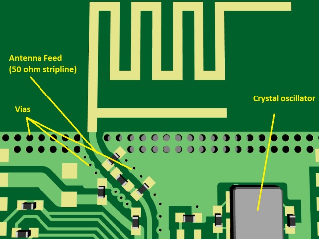
- Put component on radio frequency board in layout that reduces signal wire length and uses less vias. Put small components about important points. Short RF lines as possible and not make close to power plane traces and noise creation points
- Connect solid ground plane beneath RF traces for reducing return paths and reducing tradition and crosstalk.
- Use microstrip lines for matching the impedance of RF traces with components. Ensure trace widths and spaces fulfill impedance tolerances
- Connect shielding connectors or RF sholes to avoid RF signal leakage and reduce interference from external sources.
- After completion of layout perform test for verification operation of circuit. Use a system analyzer for measuring insertion loss and bandwidth
RF PCB vs High-Frequency PCB vs Microwave PCB
- HF waves are signals that have a frequency of 10Khz for high-frequency ranges there are long waves, short waves, super short waves, and microwaves. RF is transmitted through the transmitter and microwaves have 0.1mm to 1mm wavelengths
- HF boards are operated with signals of more than 10Khz RF with 300KHz to 300GHz, and microwave boards operate with 300MHz to 300GHz.
- All types of boards are made with materials that have good dielectric constant, dielectric losses, and thermal expansion. HF boards are made with PTFE ceramic or FR4 materials. RF boards made with high-grade PTFE such as Roers and MICrowave boards made with PTFE, PPO, and ceramic.
What is the concept of PCB layout design?
- PCB layout design is important for ensuring signal quality and avoiding electrical issues like interference and defines as radio frequency interference or electromagnetic interference. Try to avoid issues that affect the routing of traces.
RF Transmission Lines
There is need of RF components need controller impedance transmission lines that move RF capacity to IC pins to the board. These transmission lines are configured on external layers, or covered in inner layers. The rules of these transmission lines are based on details of coplane waveguide microstrip and trademark impedance.
What format is PCB layout?
- Gerber RS-274X is commonly used in Gerber format and a larger level is viewed as an accepted industry standard. The latest PCB layout tools give output in this format, older tools can be used in obsolete 274D format.
What are the uses of PCB layout?
- PCB boards are the main part of the telecommunication industry and are used for consumer devices like mobile phones and also for a structure that helps devices to operate. The telecom industry uses different types of PCB board since there are different instruments used in this field.
What is the difference between PCB schematic and PCB layout?
- The PCB schematic is a dimensional circuit design that comes with functions and connections between different components. PCB designs are 3-dimensional layouts that show components and locations when the circuit is operated.
What is the basic structure of PCB?
- PCB can come in single sides, double sides, or multilayer boards based on design and project demands.
What are the three main types of PCBs?
- Single-sided.
- Double-sided.
- Multilayer.
- Rigid.
- Flex.
- Rigid-flex.
What is RFID PCB?
- The RFID board is the main component of the RFID system. It comes with antennas, chips capacitors resistors, and other electronic components. It operated based on receiving processing and radio frequency transmission signals through certain circuit layouts.
What is the difference between RF PCB and digital PCB?
- The RD baord uses strongly controlled impedance lines and less-loss dielectric materials for maintaining signal quality for different frequencies in gigahertz. The digital board uses FR4 and affects on highspeed digital data transmission
What is the impedance matching for RF PCB?
- Impedance matching makes sure trace line dimensions propagate the effective transmission of RF signals from load to source. The dimensional transmission lines effect features impedance
What does the RF board do?
- RF circuti boards and microwave boards are used to communicate signals where there is a need to receive and transmit radio signals. Such as common uses are cell phones and radar installations.
Read also:
- PTFE PCBs: The Ultimate Solution for High-Frequency Applications
- What is Ball Grid Array (BGA) on a PCB Board
- Introduction to PCB Boards Inks, Types, Uses, & Applications
- Types of PCB Board
- Double Sided PCB Board, Construction, Working, Types & Applications
- Single Sided PCB Board, Construction, Working, Features & Applications
That is all about the RF PCB Layout if you have any further queries ask in the comments. Thanks for reading have a good day. See you in the next post.


