 Hello fellows, I hope you all are doing great. In today’s tutorial, we will have a look at Analyze Low-Frequency Response of Amplifier. For capacitively coupled amplifier if signal frequency is less than critical value then there will be an effect on voltage gain and phase shift. At less value of frequency, the reactance of the coupling capacitor becomes sufficient which causes a decrement in voltage gain and increment in phase shift.
In today’s post, we will have a detailed look at BJT and FET capacitively coupled amplifiers frequency response and related parameters. So let’s get started with Analyze Low-Frequency Response of Amplifier.
BJT Amplifiers Circuits
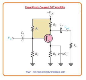
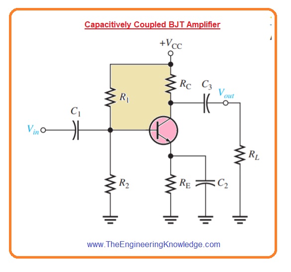
- In the below figure capacitively coupled common emitter amplifier configuration is shown.
- Suppose that coupling and bypass capacitors are ideally shorted at midrange signal frequency we can calculate midrange voltage gain with the use of the below-given equation. In this equation Rc = RCΙΙRL.
Av(mid)=Rc/r’e
- If swamping resistance RE1 is used it exits in series and then the equation will be.
Av(mid)=Rc/(r’e + RE1)
- In above figure, there is BJT amplifier that has three high pass RC circuits which affect its gain with the decrement in frequency less than midrange.
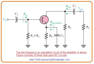
- It is shown in below less frequency ac resultant circuitry.
- The less frequency resultant circuitry retains the coupling and bypass capacitors since XC is not less to ignore when the signal frequency is very less.
- One RC circuitry is created with the input coupling capacitor C1 and input resistance of amplifier.
- The 2nd RC circuitry is created with the output coupling capacitor C3, the resistance can be seen at collector (Rout) and load resistance.
- The 3rd RC circuitry which affects the low frequency response is created with the emitter bypass capacitor C2 and the resistance seen at the emitter.
Input RC Circuit
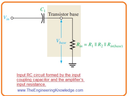
- The input RC circuitry of bipolar junction amplifier shown in first figure is created with the capacitor C1 and input resistance of amplifier and it shown below figure.
- With the decrement in signal frequency XC1 rises. It causes less voltage about the input resistance of amplifier at base terminal since further voltage is lost about the capacitor C1 and due to this overall voltage gain of amplifier deccreases.
- The base voltage of input RC ciruitry shown in above figure can be explained as.
Vbase= (Rin/√(R2in + X2C1))Vin
- As previous discuss the critical point in response of amplifier exits when the output voltage is 70.7 percent of its midrange value.
- This situation exits in the input RC ciruitry when XC1= Rin.
Vbase= (Rin/√(R2in + R2in))Vin=(Rin/√(2R2in))Vin=(Rin/(√2.Rin))Vi
Vbase=0.707Vin
- In the form of decibels.
20log(Vbase/Vin)= 20 log (0.707) = -3dB
Less Critical Frequency
- The situation where the gain is less three decibel is logically known as point of amplifer response, the net gain is three decibel lower than midrange frequency due to attenuation of input RC circuitry.
- The frequency fcl, over which this situation exits is known as less or lower critical frequency also called cutoff frequency, or lower break frequency and can be find as.
XC1=1/2pfcl(input)C1=Rin
fcl(input)=1/2ΠRinC1—-(A)
- If the resistance of input source is take into consideration then equation A will be.
fcl(input)=1/2Π(Rs + Rin)C1
Voltage Gain Roll-Off at Low Frequencies
- As we have discussed that input RC circuitry decreases the overall voltage gain of amplifier through three decibel when the frequency is decreased to the critical value fc.
- With the decrement in frequency less than fc the overall voltage gain also decreases with that.
- The rate with which voltage gain decreases with the frequency is known as roll-off.
- For every 10 time decrement in frequency less than fc there is twenty decibel decrement in voltage gain.
- Let us suppose that a frequency which is one tenth of critical frequency (f = 0.1fc).
- As XC1=Rin at fc, then XC1=10Rin at 0.1fc due to inverse relation of XC1 and f.
- The attenuation of input RC circuitry will be as.
- Attenuation=Vbase/Vin=Rin/√(R2in + X2C1)=Rin/√(R2in + (10Rin)2)
=Rin/√(R2in + 100R2in)=Rin/Rin√101=0.1
- The attenuation in decibel will be.
20 log(Vbase/Vin)=20 log (0.1) = -20 dB
What is Bode Plot
- The ten time variation in frequency is known as decade. Therefore for input RC cirucitry the attenuation is decreased by twenty decibels for every decade which the frequency reduces the critical frequency.
- It cuases the overall voltage gain to loss twenty decibles per decade.
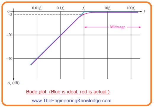
- The plot of decibel voltage gain vs frequency one semilog graph paper or logarithmic x-axis and linear Y-axis is known as Bode plot.
- The general Bode plote for input RC circuitry is shown in below figure.
- The ideal response curve is drawn in blue color. You can see that it is flat or zero decibel approaching to the critical frequency at this point the gain decrease at -20 dB/decade as denoted.
- Over the fc there are midrange frequency.
- The actual response curve is drawn in red color. Note that it reduces slowly iniating in midrange and goes tot he critical frequency.
- Frequently, the ideal response is used for simplification fo amplifier analysis.
- As above discussed value to critical frequency for which curve breaks into drop is known as -20 dB/decade lower break frequency
- Occasionally, the voltage gain roll-off of an amplifier is stated in dB/octave instead of dB/decade.
- An octave resembles to a doubling or halving of the frequency.
- For instance the increment in frequency from one hundred hertz to two hundred hertz is an octave.
- Similarly the decrement in frequency from one hundred to fifty kilohertz is also an octave.
- The rate -20 dB/decade is almost equal to rate of -6 dB/octave and the rate of -40 dB/decade is equal to the -12 dB/octave
Phase Shift in Input RC Circuit
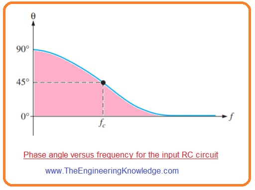
- With reduction of voltage gain the input RC circuitry also causes increment in phase shift through amplifier with the decrement of frequency.
- For midrange frequency the phase shift through the input RC circuitry is almost 0 since the capacitive reactance XC1 is almost zero ohm.
- At less frequency large values of XCq causes phase shift and the output voltage of RC circuitry generates the input voltage.
- As we know that phase angle in an input RC circuitry is define as.
θ=Tan-1(XC1/Rin)
- For midrange of frequency Xc1=0 ohm.
θ=Tan-1(0Ω/Rin)=0
- For critical frequency XC1=Rin, so
θ=Tan-1(Rin/Rin)=45
- For decade less the critical frequency XC1=10Rin, therefore
θ=Tan-1(10Rin/Rin)=84.3°
- The continuation of this procedure will result the phase shift through the input RC circuitry approaches nienty degree when frequency approaches 0.
- In below figure the graph of phase angle vs frequency is shown.
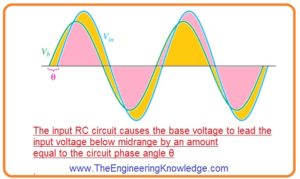
- The output is that voltage at base of transistor causes the input signal voltage in phase less the midrange it shown in below figure.
Output RC Circuit
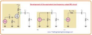
- The 2nd high pass RC cirucitry in BJT amplifer shown in first figure is created with the coupling capacitor C3 the resistance seen at the collector and load resistance as RL, is shown in below figure denoted as ‘a’.
- For determination of output resistance observing from the collector the transistor is operating as an ideal current source and upper part of RC is at ac ground shown in figure denoted as ‘b’.
- So applying thevenin the left side of capacitor C3 generates an resultant voltage source equal to the collector voltage and series resistor identical to RC as shown in figure denoted as c.
- The less critical frequency of this output RC circuitry is given as.
fcl(output)= 1/2Π(RC+RL)C3
- The effect of output RC circuitry on the amplifier voltage gain is like the input RC circuitry.
- With the decrement of signal frequency XC3 increases.
- It causes less voltage loss about the load resistance since large voltage is loss about the capcaitor C3.
- The signal voltage is decreased with the factor of 0.707 when frequency dereases to the less critical value fcl. This correspondent to three dB decreases in voltage gain.
Phase Shift in Output RC Circuit
- The phase angle int output RC circuit is given as.
θ=Tan-1XC3/(RC+RL)
- θ is zero for midrange frequency and approaches to ninety degree as frequency approaches zero.
- For critical frequency fc the phase shift is 45 degree.
Bypass RC Circuit
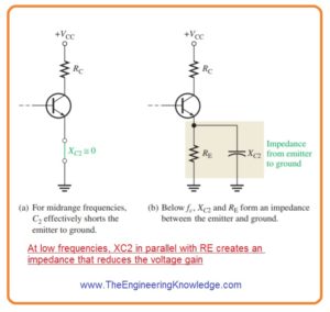
- The 3rd RC circuitry which affect the less frequency gain of bipolar junction amplifier in first figure now consists of bypass capacitor C2.
- It shown in below figure denoted as ‘a’ for midrange frequency it is supposed that XC2=0Ω shorted the emitter with the ground so amplifier gain is Rc>r’e.
- With the decrement in frequency XC2 increases and there is no sufficient less reactance to position the emitter at ac ground it shown in above figure denoted as b’.
- Since impedence from emitter to ground rises the gain reduces.
- In this condition Re in the equation Av=Rc/(r’e + Re) is substituated with the impedance created with the resistance RE in parallel with the XC2.
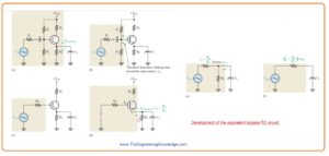
- The bypass RC circuitry is created with the capacitor C2 and resistance seen at the emitter Rin(emitter), as shown in figure denoted as a’.
- The resistance connected with emitter can be calculate with the following procedure.
- In figure denoted as b’ thevenin theorem is applied starting from base of transistor to the input source Vin.
- It make equivalent resistance Rth ad equivalent voltage source Vth(1) connected in series with the bas as shown in figure denoted as c’.
- The resistance seen at the emitter is find with the equivalent source shott circuited it shown in figure denoted as d’.
Rin(emitter)=r’e+Ve/Ie=r’e+Vb/βacIb=r’e+IbRth/βacIb
Rin(emitter)=r’e+Rth/βac
- Observing from capacitor C2 r’e+Rth/βac is in parallel combination with the resistance RE it shown in figure denoted as e’.
- By applying thevenin therom again we have equivalent RC circuitry shown in figure denoted as f’.
- The lower critical frequency for this resultant bypass RC circuitry is given as.
fcl(bypass)=1/2Π[(r’e+Rth/βac)ΙΙRE]C2
- If we use swamping resistance the final equation for Rin(emitter) will be.
Rin(emitter)=r’e + RE1+Rth/βac
FET Amplifiers
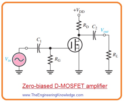
- The zero biased D-MOSFET amplifier configuration with capacitive coupling on both input and output sides is shown in below figure.
- The midrange voltage gain of zero biased amplifier is given as.
Av(mid ) = gmRd
- It is the gain for frequency is large enough that capacitive reactances are almost 0.
- The amplifier shown in above figure has only 2 high pass RC circuitry which affects its low frequency response.
- One RC circuitry is crated with the input coupling capacitor C1 and input resistance.
- The second circuitry is created with the input coupling capacitor C2 and output resistance connected with the drain.
FET Amplifiers Input RC Circuit
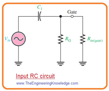
- The input RC circuitry of field effect transistor amplifier shown in above figure is created in below figure.
- As we discussed that in BJT amplifier the reactance of input coupling capacitor rises with the frequenvy decrement.
- When XC1=Rin the gain is three decibels less that its midrange vlaue.
- The lower critical frequency is given as.
fcl(input)=1/2ΠRinC1
- The input resistnac is givne as.
Rin=RGΙΙRin(gate)
- In this equation Rin(gate) is find from datasheet reading.
Rin(gate)=ΙVGS/IGSSΙ
- The lower critical frequency is given as.
fcl(input)=1/2Π(RG || Rin(gate))C1
FET Amplifiers Output RC Circuit
- The 2nd RC circuitry which effects the low frequency response of field effect transistor amplifier is created with the coupling capacitor C2 and output resistance connected with the drain is shown in below figure denoted as a’.
- The load resistance Rl is added. For BJT the field effect transistor is operated as current source and the upper part of resistance RD is ac ground is shown in above figure denoted as b’.
- The thevenin resultant on left side of C2 is shown in figurer denoted as c.
- The lower critical frequency for this RC circuitry is given as.
fcl(output)=1/2Π(RD +RL)C2
- The effect of output RC circuitry on the voltage gain of amplifier less than the midrange is like the input RC circuitry.
- The circuitry with the largest critical frequency dominates since it is that ist causes the gain to roll off as frequency is less than its midrange values.
- The phase angle in less frequency output Rc circuitry is given as.
θ=Tan-1XC2/(RD +RL)
- Again we say that at critical frequency the phase angle is fourty five degree and approaches nienty degree when frequency is approaching 0 degree.
- Though initiating from critical frequency the phase angle reduces from fourty five degree and becomes very less as frequency increases.
Total Low-Frequency Response of an Amplifier
- Till now we have discussed seperately the high pass RC circuitry which affect a voltage gain of BJT or FET amplifier at less frequency now let us discuss totoal effect of 3 RC circuitry in BJT amplifier.
- Every circuitry has cirtical frequency calculated with the R and C parameters,
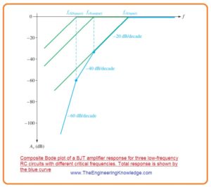
- The critical frequency of 3 RC circuitry are not all same.
- the critical frequency of one RC circuitry is larger than then other 3, then it is dominant RC circuitry.
- The dominant circuitry find the frequency at which the total voltage gain of amplifier start to decrease at -20 dB/decade.
- The other circuits every causes an extra -20 dB/decade roll off less their respective critical frequency.
- To obtain a good result of less frequency we construct a Bode plot in below figure.
- It displays the superimposed ideal responses for 3 RC circuitry in green lines of BJT amplifier.
- In this example every RC circuitry has different critical frequency. The input RC circuitry is dominant in this condition and bypass RC circuitry has less fc.
- The ideal total response is shown in blue color lines.
- At this point is happen that. With the decrement in frequency from mirange the ist break point occurs at critical frequency of input RC circuitry, fcl or input and gain starts to decrease at -20 dB/decade.
- This constant roll-of rate continues till the critcal frequency of the output RC circuitry fcl (output) is obtained.
- For this brak point the output RC circuitry added another -20dB/decade to create a total roll-off of -40dB/decade.
- this constant -40dB/decade roll-off continous till the critical frequency of bypass RC circuitry is obtained.
- The bypass RC circuitry added further -20dB/decade at this break point creating the gain roll-off at -60dB/decade.
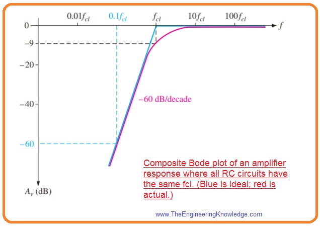
- If all RC circuitry has similar value of critial frequency the response curve has one break point at that value of fcl, and the voltage gain roll off at -60dB/decade less this value is shown in below figure with the ideal curve in blue color.
- In real the midrange voltage gain deos not extended to the dominant critical frequency but is -9dB less the midrange voltage gain is shown in above figure in red curve.
Read also
- Amplifier circuit using LA4440 IC
- Difference Between Inverting and Non-Inverting Amplifier
- Introduction to MPSA06 NPN Amplifier Transistor
- Introduction to 2SC1345 NPN Amplifier Transistor
- Analyze Multistage Amplifiers Frequency Response
That is detailed post about Analyze Low-Frequency Response of Amplifier if you have any query ask in comments. Thanks for reading. Have a good day.



once again a great post
I lately came across your blog and have been studying along. I believed I would leave my initial remark. I don???ê?èt know what to say except that I have relished reading. Pleasant blog. I will maintain visiting this blog extremely typically.