 Hello fellows, I hope you all are doing great. In today’s tutorial, we will have a look at Analyze High Frequency Response of Amplifier.In the previous tutorial low frequency response of amplifier we have discussed that coupling and bypass capacitors has an effect on the voltage gain of amplifier at les frequency at a point where reactances of bypass and coupling capacitor are important.
In midrange of amplifier the effects of capacitors are negligible and can be ignored. If frequency rises to such point where the inner capacitance of transistor has sufficiently effect on the gain. In today’s post, we will have a detailed look response of high frequency for both BJT and FET amplifiers. So let’s get started with Analyze High-Frequency Response of Amplifier.
Analyze High-Frequency Response of Amplifier
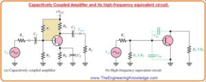
- The high-frequency ac resultant circuitry for the BJT amplifier circuit shown in figure denoted as a’ is shown in figure denoted as b’.
- We can note that coupling and bypass capacitors are operating as short circuit and do not exit in a resultant circuit.
- The inner capacitances Cbe and Cbc, which are substantial only at high frequencies, exist in this circuit.
- Cbe is also known as input capacitance and denoted as Cib, and Cbc is also known as output capacitance and denoted as Cob. Cbe is mentioned on the datasheet at a specific value of VBE.
- Frequently, on datasheet Cib is denoted as Cibo and Cob as Cobo. The ‘o’ last letter in the subscript denotes the capacitance is calculated with the open base.
- For instance, a 2N2222A transistor has a Cbe of twenty-five picofarad VBE 0.5 Volts dc, IC=0, and f=one MegaHertz.
- With that Cbc is denoted at a specific value of VBC. The 2N2222A has a maximum Cbc of eight picofarads at VBC 10 Volts dc.
Miller’s Theorem in High-Frequency Analysis
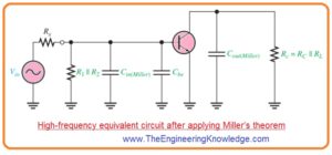
- After application of Miller theorem on the circuit shown in above figure denoted as b’ and with use of midrange voltage gain will get a circuitry that can be discussed for high frequency response.
- Observing from the signal source the capacitance Cbc seems in the Miller input capacitance from base to ground.
Cin(Miller)= Cbc (Av + 1)
- Cbe just seems as a capacitance to ac ground, it shown in below figure in parallel combination with the Cin(Miller).
- Observing from the collector Cbc seems in the Miller output capacitance from collector to ground.
- It shown in above figure the Miller output capacitance looks in parallel combination with resistance Rc.
Cout(Miller)= Cbc((Av + 1)/Av)
- These 2 Miller capacitances make high frequency input RC circuitry and high frequency output RC circuitry.
- These 2 circuitry are different from the less frequency input and output circuitry that operate like high pass filters since the capacitances are to be grounded and so behaves as low pass filters.
- The corresponding circuitry shown in above figure is an ideal model since stray capacitances which is due to interconnections of circuitry are ignored.
BJT Amplifiers Input RC Circuit
- For large value of frequency input circuitry is shown in below figure denoted as a’. in this circuit input resistance at base terminal of transistor since the bypass capacitor is shorted with the emitter to ground.
- By joining the Cbe and Cin (Miller) in parallel combination and changing position we will have simple circuit as shown in figure denoted as b’.
- After that by applying the Thevenin theorem the circuitry to the left side of capacitor as shown the input RC circuitry is decreased to resultant circuit shown in figure denoted as c’.
- With the increment in frequency the capacitive reactance get decreases.
- It causes the signal voltage at base to reduce therefore voltage gain of amplifier reduces.
- The cause for this is that capacitance and resistance behaves as voltage divider and frequency rises, further voltage is decreased about the resistance an less voltage loss occur about the capacitance.
- For critical frequency the gain is three decibels lesser then midrange value.
- The upper critical large or high frequency of input circuitry is that frequency over which the capacitive reactance is equal to total resistance.
XCtot = Rs││R1││ R2 ││βac r’e
So
1/2πfcu (input)Ctot= Rs││R1││ R2 ││βac r’e
fcu(input)=1/ 2π(Rs││R1││ R2 ││βac r’e) Ctot
- in this equation Rs is resistance of signal source and Ctot =Cbe +Cin(Miller).
- As frequency is larger than the fcu(input), the input RC circuitry causes the gain to roll off at with the rate of low frequency response.
Phase Shift of Input RC Circuit
- Due to output voltage of high frequency input RC circuitry is about the capacitor the output of cirucitry is lagging the input.
- The phase angle is defined as.
Θ=tan-1 (Rs││R1││ R2 ││βac r’e)/ XC(tot)
- For critical frequency the phase angle is forty five with the signal voltage at the base of transistor lags the input.
- As frequency rises over the fc the phase angle greater than forty-five degree and approaches to 90 degree when the frequency is adequately large.
BJT Amplifiers Output RC Circuit
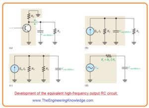
- The large frequency output RC circuitry is created with the Miller ouput capacitance and resistance seen at the collector, it shown in figure denoted as a’.
- For calculation of output resistance the transistor is behaves as a current source or open cirucit and 1 end of RC is efficiently ac ground, it shown in figure denoted as b’.
- By reordering the position of the capacitance in the figure and applying Thevenin theorm to the circuit from left side as shown in figure denoted as c’ we have resultant circuitry shown in figure denoted as d’.
- The corresponding output RC circuitry contains a resistance equal to the parallel joining of RC and RL in series with a capacitance which is calculated with the application of Miller formula.
Cout(Miller)= Cbc((Av + 1)/ Av)
- If the value of voltage gain is ten this formula will become.
Cout(Miller)= Cbc
- The value of upper critical frequency for the output circuitry is measured this equation. Here Rc = RC ││RL.
fcu(output)=1/ 2πRcCout(Miller)
- like the input RC circuitry the output RC circuitry decreases the gain by three decibels for the critical frequency.
- When frequency is larger than critical value the, the gain decreases at a -20 dB/decade rate. The phase angle for the output RC circuitry is given here,
Θ=tan-1(Rc/ XCout(Miller)
FET Amplifiers
- The tactic for the high-frequency analysis of field effect transistor is like to the bipolar junction transistor.
- The main difference is the properties of the inner field effect transistor capacitances and the calculation of the input resistance.
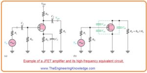
- Below figure denoted as a’ shows a junction field effect transistor common source amplifier configuration we will use this configuration to discuss the high frequency analysis for FET amplifier.
- In figure denoted as b’ the high frequency resultant circuitry of FET amplifier is shown.
- Note that coupling and bypass capacitors has ignorable value of capacitances and are taken to be short circuit.
- The inner capacitances Cgs and Cgd seem in the correspondent circuitry since their reactances are important at high frequencies.
Values of Cgs, Cgd, and Cd
- Field effect transistor datasheet usually not have values of Cgs, Cgd, or Cds.
- In its place, 3 other values are frequently stated since they are easy to find.
- Which are Ciss, the input capacitance, Crss, the reverse transfer capacitance, and Coss, the output capacitance.
- Due to the producer’s technique of calculation, the subsequent relations permit you to find the capacitor values required for analysis.
Cgd =Crss
Cgs=Ciss -Crss
Cds =Coss -Crss
- Coss is not stated as frequently as the other values on datasheets.
- Occasionally, it is denoted as Cd(sub), the drain-to-substrate capacitance.
- In conditions for which values is not given you should suppose value or ignore Cds.
Application of Miller Theorem
- Miller theorem is used in similar way for field effect transistor inverting amplifier for high frequency analysis as used for bipolar junction amplifier.
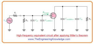
- Observing from the signal source in above figure denoted as b’, Cgd efficiently seems in the Miller input capacitance, that is given below.
- Cin (Miller) = Cgd (Av + 1)
- Cgs just seems as a capacitance to ac ground in parallel combination with Cin(Miller), is shown in below figure.
- Observing from the drain Cgd efficiently looks in the Miller output capacitance from drain to ground in parallel combination with Rd, shown in above figure.
Cout(Miller)= Cgd((Av + 1)/Av)
- These 2 Miller capacitances These two Miller participate in high frequency input RC circuitry and circuit and a high frequency output RC circuitry.
- Both of these are low-pass filters, that causes large phase.
FET Amplifier Input RC Circuit
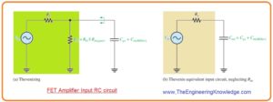
- The high frequency input circuitry creates a low pass category of filter and is shown in below figure denoted as a’
- As value of RG and input resistance at gate of field effect transistor is large the regulatory resistance for the input circuitry is the resistance of the input source as long as Rs<<Rin.
- It is due to Rs looking in parallel combination with resistance Rin after application of Thevenin theorem.
- The resultant input RC circuitry is shown in figure denoted as b’. The upper critical frequency for the input circuitry is given as,
fcu(input)=1/2πRsCtot
- here Ctot= Cgs+ Cin(Miller) = The input RC circuitry makes a phase angle is given here.
Θ=tan-1(Rs/XCtot)
- The effect of input RC circuitry is to decrease the midrange gain of amplifier by three decibel at critical frequency and causes the gain to reduce a -20 dB/decade over fc.
FET Amplifier Output RC Circuit
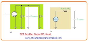
- The high-frequency output RC circuitry is created with Miller output capacitance and the output resistance observing in at the drain, is shown in below figure denoted as a’.
- For BJT the field effect transistor is operating as current source.
- After application of Thevenin theorem we have resultant output RC circuitry containing of resistnace RD in parallel combination with RL and an corresponding output capacitance.
Cout(Miller)= Cgd((Av + 1 )/Av )
- This correspondent output circuitry is shown in Figure denoted as b’ the critical frequency of the output RC lagging circuitry is given as.
- fcu(output)=1/2πRdCout(Miller)
- The output circuitry creates a phase shift given here.
Θ=tan-1(Rd/XCout(Miller) )
Total High-Frequency Response of an Amplifier
- As we have observe that 2 RC circuitry make with the inner transistor capacitance effect the high-frequency response of BJT and field effect transistor.
- As the frequency rises and approaches the highest point of its midrange values, one of the RC circuitry will causes the gain of amplifier to drop off.
- The frequency over which it happens is the dominant upper critical frequency, which is less the 2 upper upper critical high frequencies.
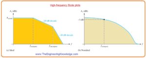
- In figure denoted as a ideal frequency Bode plot is shown.
- It displays the first break point at fcu(input) here voltage gain starts to roll off at -20 dB/decade,
- For fcu(output), the gain starts reducing at -40dB/decade since every RC circuitry is giving a roll-off.
- Figure denoted as b’ shows a non ideal bode plote in this case voltage gain is less than the midrange fcu(input).
- Other options are that the output RC circuitry is leading or both circuitry have the same critical frequency
That is detail tutorial about High Frequency Response of Amplifier if you have any question ask in comments. Thanks for reading. have a good day.


