 Hello friends, I hope you all are doing great. In today’s tutorial, we will have a look at Transistor DC Operating Point. An operating point of an instrument is called bias point, Q-point or quiescent point. It is the value of DC voltage or current at the specific terminal of an active device such as a transistor when there is no input signal is provided.
A transistor should be correctly biased with dc source to function as a linear amplifier. The dc operating point should be set such that signal variation at the input is amplified and correctly shown at output connections or terminals. In today’s post, we will have a detailed look at the transistor dc operating point with detail, its circuit, and some related parameters. So lets get started with Transistor DC Operating Point.
Transistor DC Operating Point
DC Bias
- The bias makes the dc operating point for accurate linear amplifier operation.
- If an amplifier circuit is not biased with accurate dc voltage at input and output then it will be in saturation or cutoff region when the input voltage is provided.
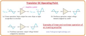
- The below figure displays the effect of proper and improper dc biasing of an inverting amplifier circuitry.
- In the first circuit denoted as (a) the output signal is amplified according to the input with an inverted waveform that indicates that it is out of phase with the input signal.
- The output signal moves over the dc bias level of output that is VDC(out).
- Inappropriate biasing can cause distortion in the output, as shown is shown in the circuit denoted as (b) and (c).
- (b) part discusses the limiting of the positive part of output voltage as a consequence of a Q point close to the cutoff.
- (c) the circuit explains the limiting of a negative part of the output signal as Q point is close to saturation.
Graphical Analysis
- In below circuit transistor is biased with the VCC and CBB to get specific values of IE, IC, IB and VCE.
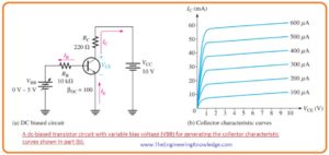
- For transistor collector characteristic curves are also shown in figure we will use all these curves for graphically explanation the effect of dc bias.
- add picA dc-biased transistor circuit
- In below figure take three values for base current and will see what effect will be on collector current and VCE.
- First of all, VBB is varied to generate a base current as shown figure denoted as (a).
- As IC = βDC IB and IC are twenty milliamperes.
VCE = VCC – ICR
=10 V – (20 mA)(220Ω)
10 V – 4.4 V= 5.6 V
On a graph of figure denoted as (a) is Q1.
- In figure denoted as (b) VBB is enhanced to generate a base current of value 300uA Ic of thirty milliamperes.
VCE = 10 V – (30 mA)(220Ω)
=10 V – 6.6 V = 3.4 V
- The Q point for this state is shone on graph as Q2.
- In figure denoted as (c) VBB is increasing to give a base current of 400uA and collector current of forty milliamperes.
VCE = 10 V – (40 mA)(220Ω)
=10V – 8.8 V=1.2 V
DC Load Line
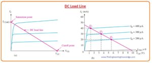
- The transistor circuitry dc operation can be explained through the graph by making dc load line.
- It is a straight line constructed on the characteristic curves from the saturation point where IC =IC(sat) on the x-axis as denoted (a) in the figure.
- The load line is measure by the exterior circuitry not through the transistor itself that is explained by the characteristic curve.
- In below figure the equation of collector current is given as.
IC= (VCC – VCE)/ RC
= (VCC/ RC)- (VCE/ RC)
= – (VCE/ RC)+ (VCC/ RC)
=- (1/ RC) VCE +(VCC/ RC)
- It is equation os straight line with the slope of -1/RC, with x intercept of VCE=VCC and y intercept of VCC=RC that is IC(sat).
- The point at which where load line crosses the characteristic curve denoted the Q point for that specific value of base current.
- The below figure describes the Q point on load line for every value of the base current shown in the above figure.
Transistor Linear Operation
- The area along the load line consisting of all points among saturation and cutoff is normally recognized as the linear region of the transistor’s operation.
- As transistor is working in this area or region the output voltage is ideally linear regeneration of input.
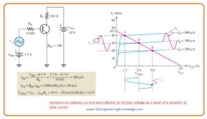
- An example of linear operation of a transistor is shown in below figure. AC parameters are denoted as lowercase italic subscripts.
- Suppose that ac voltage Vin is carrying on VBB due to that base current changes 100uA in the form of sine waveform above and below its point value of three hundred uA.
- Due to that IC change ten milliampere above and below its q point value of thirty milliampere.
- As a consequence of the change in IC, the collector to-emitter voltage changes 2.2 V over its Q point of 3.4 volts.
- Point A on load line in Figure resembles to the positive maximum of the input sine waveform.
- Point B is corresponding to the negative extreme and Q point resembles to the 0 value of sinusoidal as shown.
- VCEQ, ICQ, and IBQ are dc Q points without input sine waveform.
Waveform Distortion
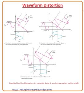
- As above denoted that over specific input signal the position of load line limit or clipped the one peak of Vce waveform as define in the figure denoted as a and b.
- In every point, an input voltage signal is high for the position of Q point and running the transistor into the cutoff or saturation for input waveform.
- When bot extremes or peaks are clipped or limited as shown in figure denoted as ‘c’ transistor is operating in cutoff and saturation regions with a large input signal.
- When only post extreme of the wave is clipped or limited transistor is operating in the cutoff region, not in saturation.
- When a negative peak is clipped or a limited transistor is operating in saturation, not in the cutoff region.
So, friends, it is a detailed post about dc operating point if you have any further queries about dc operating point of transistor ask in comments.


