 Hello, friends welcome to new post. Today we will learn the Introduction to TYN268PN. It is integrated of a line switching board comprised of controller circuitry with a power switch in a single casing. There is a need of fewer exterior modules to run the main circuits.
Here we will get details about working, features, and some related parameters. So let’s get started with Introduction to TYN268PN.
Introduction to TYN268PN
- The TYN268PN integrated circuitry is compatible with seven hundred volts power MOSFET, a current limiting circuit and the HiGH volts switching current source is compatible in one casing.
- The operating current is given to the drain pin to reduce the bias windings and other related circuits.
- It consists of small switch modules that work as auto-restarted sense line limited volts and frequency changes.
- Its simplest structure reduces the audio frequency elements through just on and off modes to reduce the noise through a taped transformer.
- It comes with an auto-restart circuit that restricts output energy through fault conditions like when a short circuit exits
- It consists of line sense resistance outer get to control a line under volts that reduces power down changes resulting by the discharge of input storage capacitors existing in standby circuits.
- For elimination, the quasi-peak and average EMI one thirty-two-kilo hertz frequency is used

TYN268PN Features
- The main features of TYN268PN are explained here
- Its output power value is twenty-three watts at two-thirty volts AC and fifteen watts for eighty-five volts AC.
- The duty cycle is sixty-five percent
- Consists of built-in circuits to reduce the noise.
- Its high tolerance and fewer temperature changes reduce its cost
- Its lower cost makes it a replacement of large-size regulated liners
- Its current limit circuit and thermal protection enhance safety
- The operating temperature is minus forty to one fifty centigrade
- Its switching frequency is one thirty-two kilohertz
| Features | Details |
| Mount | Through Hole |
| Mounting Type | Through Hole |
| Package | 8-DIP, 7 Leads |
| Number of Pins | 8Pins |
| Weight | 2.26799g |
| Operating Temperature | -40°C to 150°C TJ |
| Packaging | Tube |
| Series | TinySwitch |
| JESD-609 Code | e3 |
| Pbfree Code | yes |
| Part Status | Not For New Designs |
| Moisture Sensitivity Level | 1 |
| Terminations | 7Terminations |
| ECCN Code | EAR99 |
| Terminal Finish | Matte Tin |
| Max Power Dissipation | 23W |
| Terminal Position | DUAL |
| Internal Switch(s) | Yes |
| Fault Protection | Current Limiting, |
| Max Duty Cycle | 68 % |
| Max Supply Voltage | 265V |
| Drain to Source Resistance | 5.2Ohm |
| Duty Cycle | 65% |
| Output Isolation | Isolated |
| Min Supply Voltage | 85V |
| Height | 3.68mm |
| Length | 9.83mm |
| Width | 6.6mm |
| REACH SVHC | No SVHC |
| Radiation Hardening | No |
| RoHS Status | RoHS Compliant |
| Lead Free | Lead Free |
| Topology | Flyback |
| Control Technique | PWM |
| Switcher Configuration | SINGLE |
Technical Specifications
| Output Power (Max) – Open Frame, 230V | 23.00 W |
| Breakdown Voltage | 700 V |
| Temperature – Operating (Min) | -40 °C |
| Temperature – Operating (Max) | 150 °C |
| IC Package | DIP-8B |
| Mounting Type | Through Hole |
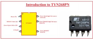
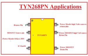
TYN268PN Pinout
- The Pinout of this device is explained here
- BP is pin 1 used as a bypass for the inner 5.8 volts regulator
- pins 2,3 are sources pins of MOSFET
- pin 4 is EN used to enable the IC during the undervolted condition
- pin 5 is the Drain pin of MOSFET
- Pins 7, 8 are Mosfet High volts sources that return pinout

TYN268PN Applications
- The main applications of TYN268PN are explained here
- It used in large input volts flyback converter circuits
- Battery backup charges consist of this board
- Off-line power converters used this IC
- It is used in mobile phones and laptop charges
TYN268PN Working
- The circuit creation of an offline converter comes with the difficult task of measuring different components, safety must considered first. ICs TYN268PN are used for making work easy through integration control components and power switches on single integrated circuits.
- Some other components are used such as a transformer, and a passive component. here circuit you can see

- TYN268PN works like high-power MOSFET used at low winding of the transformer. Just two additional pins are used to bypass the power supply and the UV pin that used as a feedback pin.
- The feedback pin is an optocoupler that gets on when the output zener diode crosses the breakdown voltage.
- The RC circuit is connected to the drain of the IC to prevent voltage spikes from damaging the inner power switch.
- IC comes with an inner 6.4 volts zener diode for clamping drain-source voltage at safe values.
- The current through the switch is limited to 500mA.
What is the equivalent of TNY268PN?
- TNY278, NCP1014, LNK304, LNK306, NCP1702,
Read also
That is all about the TYN268PN all details has explained further you want to know ask in the comments. Thanks for reading have a good day see you in the next post.


