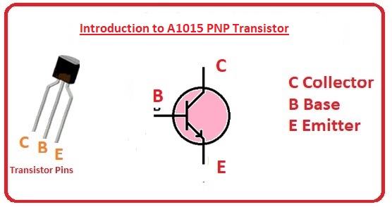
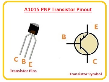
 Hello readers, welcome to a new post. In this post, we will discuss an Introduction to the A1015 PNP Transistor. A transistor is a very commonly used electronic device used in different projects, such as amplifiers and switches. Its configuration has three pinouts: the emitter, the base, and the emitter.
Its main types are PNP and NPN. in NPN transistor there is one N part among the two P types of material. While in NPN there is two P regions and one N. Both has their own features and applications. Here we will have detailed overview about the A1015 PNP transistor features working and some other parameters. Here i further want to mentioned that if you are workings on projects where you want to used this module and has make circuit on the PCB board of your project. Facing difficulty to make it i will suggest you make contact to the most reliable and economically sound PCB provider. That offers the PCB services with reasonable prices with that they also have the high professional team of engineers and technician that will help you to make your project very accurately according to your requirements with reasonable prices. That service provider is PCBWAY that located in china and operating all over the world to their clients. their business objective is to be the most professional PCB producer for prototyping and low-volume production to work with in the world. With more than a decade in the field, PCBWAY is committed to meeting the requirements of their clienteles from different industries in footings of quality, delivery, cost-effectiveness and any other demanding requests. As one of the most experienced PCB manufacturers and SMT Assemblers in China, they pride themselves to be your best business partners as well as good friends in every aspect of your PCB needs

what is A1015 PNP Transistor
- The short ball makes soldering the 1015 PNP transistor simple. It is used in different circuits and projects.
- There is a need for a 3.5mm ferrite spike for the transistor wafer exposed at 125 degrees temperature, which is about 0.8 million°C.
- The curing method for transistors with PNP is also the same as the local crystal.
- It is used for circuits where amplification is needed. It is also part of the switch.
- The working operation is for active mode for sound frequency amplification because it uses three working modes: active, cutoff, and saturation.
What makes transistors electrically conductive?
- Transistor comes with many electrons for releasing light. That needed power since emitted electrons moved with speed.
- The A1015 PNP transistor is not large in size compared to a pencil tip.
- Transistors use high energy for releasing signals. Since ions do not remain in direct connection, that is used for transmitting signals. It is possible for a transistor to release line flow.
- 3 transistors are connected at that line that avoids gaps. Transistors are affected by temperature since they store charged ions.
- The high ions are charged with more signals for transistor paths that are released.
A1015 Features
| Features | Details |
| Type | PNP |
| Maximum Collector Power Dissipation | 0.4 W |
| High Voltage and High Current | Vceo = 50V, Ic = 150mA |
| Low Noise | 1 dB |
| Case Material | Molded Plastic |
| DC Current Gain | 70 to 400 |
| Collector-Base Voltage | -50 V |
| Collector-Emitter Voltage | -50 V |
| Emitter-Base Voltage | -5 V |
| Maximum Collector Current | -150 mA |
| Operating Junction Temperature | 150 °C |
| Transition Frequency | 80 MHz |
| Complementary Transistor | 2SC1815 |
A1015 Absolute Maximum Ratings
| Features | Symbol | Rating | Unit |
| Collector-Base Voltage | VCBO | -50V | Volts |
| Collector-Emitter Voltage | VCEO | -50V | Volts |
| Emitter-Base Voltage | VEBO | -5V | Volts |
| Collector Current | IC | -150mA | MA |
| Power Dissipation | PC | 400mW | MW |
| Junction Temperature | Tj | 150°C | Celsius |
A1015 PNP Transistor Construction
- • The transistor is made with 5 layers of conductors that are 6 nm thick and come with a lead aluminum inlet layer, electrode layers that are 12 nm thick, and a semiconductor insulator and thin capacitor layers.
Working of A1015 Transistor?
- Here is an LED flasher circuit made where the 2SA1015 transistor is used, which has capacitors C1 and R1 for the frequency generator to the Q1 transistor that is working as a switch for Q2.
- Q2’s main function is to increase current.
- Capacitor C to R2 and LED, Q1 operates until voltage losses increase about C1. As a result, the Q2 conducts and the current flows in the LED, and it will be ON.
- When C1 is discharged through R1 for some time, C1 discharge will have no pressure for the bias base pin of Q1.
- So Q1 stopped working, which also affected the working of Q2. So, the lead gets off, and C1 starts working, and this process continues. As a result of the ON and OFF of the LED, we can see it as a flasher.
A1015 Features
- Operating temperature is minus fifty-five to one hundred fifty.
- VBE is 1.45 dc volts.
- VBE is 1.1 dc.
- Gain value is four hundred.
- Collector power dissipation is four milliwatts.
- It constructed with material molded plastic
- Noise value is one decibel.
- Value of power dissipation is 0 watts.
- It is a category of PNP transistor.
A1015 Transistor Equivalent
| Transistor | Description |
| NTE290A | Silicon NPN Transistor |
| 2SA495 | Silicon PNP Transistor high-frequency |
| 2SA561 | Silicon PNP Transistor |
| 2SA564A | Silicon PNP Transistor |
| 2SA573 | Silicon PNP Transistor |
| 2SA675 | Silicon PNP Transistor |
| 2SA705 | PNP Transistor |
| 2SA850 | PNP Transistor |
| 2SA999 | PNP Transistor |
| KTA1015 | PNP Transistor |
| BC212 | PNP Transistor |
| BC257 | PNP Transistor |
| BC307 | PNP Transistor |
| BC557 | PNP Transistor |
| 2N3494 | PNP Transistor |
| 2SA781 | PNP Transistor |
| KT3108A | PNP Transistor |
| 2SA1015 | PNP Transistor |
| 2SA1267 | PNP Transistor |
| 2SB560 | Silicon PNP |
| KSA1015 | PNP Transistor |
| KTA1266 | PNP Transistor |
A1015 PNP Transistor Applications
- Main applications are listed here
- It is the part of LED flasher circuits
- used as amplifier
- work as switch
- Employed in Darlington pairs