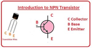
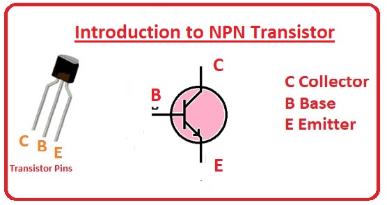
 Hi, readers welcome to the new post. In this post, we will describe the Introduction to NPN Transistor. In the NPN transistor, there is 2 N and one P semiconductors material are assembled. P is in med and N is at two ends. Generally, the transistor is used in the switching and amplifier process.
It has three main pinouts that are emitter, base, and collector. These components are linked in the circuit where it is used and performs respective functions. here we discuss different parameters related to NPN transistors. So let’s get started
What Is an NPN Transistor?
- One of the most important transistor concepts is the NPN transistor. The principal purpose of the NPN transistor is to reduce power consumption. Here, the primary focus is on minimizing electrical resistance.
- As a result, more electrons or holes are created. As these charges move through the junction, they can attract each other and be accelerated into the p-type semiconductor. This then electrically activates the device.
- In a p-n junction, p electrons are attracted to n holes. As a result, electrons move fastly than holes in semiconductors materials
- It causes a decrement in resistance value. To get this decrease in resistance semiconductor material has less operating voltage.
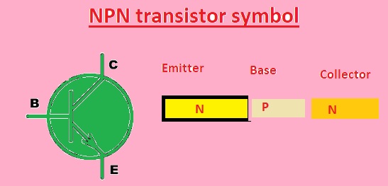
NPN transistor symbol
Construction of NPN Transistor
- NPN transistor is constructed with three layers of semiconductors material that are emitter-base and collector. Semiconductors material is normally silicon but other material like germanium can also be used
- The emitter is doped through impurities to increase free electrons and an N-type semiconductor is created. The base that is existing between the emitter and collector is very small and light-doped with impurities to make P-type material. Collector also doped as N material.
- The transistor is created by sandwiching a thinner P-type base layer among thick emitter and collector that are N-doped. If a small current is given at the base terminal it regulates the flow of electrons emitter to the collector.
- The current flowing in the base produces a larger current to move from emitter to collector. This is due to the base-emitter junction in forward biased permitting electrons to flow in the emitter to the base easily. When electrons move in the base move to collectors that are reverse-biased and attract the electrons
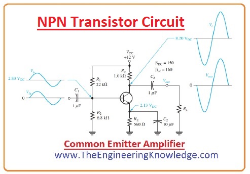
NPN Transistor Circuit
- The NPN transistor is used in differnt circuits configuration on the bases of project demand. Its common to use circuit configuration is a common emitter configuration used for signal amplification
- In this configuration, the emitter is attached to the ground collector and is connected to a positive power source, and the base is linked to the input signal source. The load resistor is connected to a collector to control output volts.
- If small input volts is applied to the base it regulates the current flow from the emitter to a collector that amplification of the input signal.
- The load resistor is connected to the collector terminal and transforms amplified current in the voltage signal.
- The common emitter configuration provides the high voltage gain and mid-level curent gain so it is used as an amplifier. Though it has low input impedance and high output impedance that has an effect on the frequency circuit response.
- With common emitter configuration, other types of NPN transistor circuit configurations are used that are the common base that has low voltage gain and high curent gain and common collector configuration it another circuit. That is a high input impedance and low output impedance.
Operating Mode of Transistor
There are three modes of operation transistors that are listed here
- Cut-off mode
- Saturation mode
- Active mode
- Transistors operate in three modes that are active, saturation, and cut-off modes. The operating modes of transistors are defined on the basis of the voltage given to the transistor.
Active mode:
- In active mode transistor work as an amplifier. The base-emitter junction is forward-biased permitting the small current to flow from base to emitter. This current regulates larger current passing through the collector to emitter and amplify the output signal
Saturation Mode
- Transistor operates as a switch in saturation mode. The base-emitter junction is forward-biased causing a larger current to flow from the collector to the emitter. The transistor operating is in saturation when the collector curent has the highest value and more increases in base current do not cause any further increase in collector current.
Cutt off Mode
- The transistor is in an off state for cutoff mode. The base-emitter junction is in reverse biased presenting current to flow from base to emitter. As a result, the collector current is very small and the transistor operates like open circuitry.
- The operating mode of the transistor can be regulated by changing the voltage given at transistor terminals. The base-emitter voltage is used for control the operating mode of the NPN transistor, but collector-emitter voltages find magnitude of the output signal in the active mode
How Does an NPN Transistor Work?
- If you think about the design of the transistor from the semiconductor material perspective, you will begin to realize that the outer material is the wire.
- At the inner part of the transistor, there is insulator material and P material and here electrons and holes that are carriers exist.. These two materials sandwich a layer of p-type semiconductor, where the majority of the holes reside.
- It is not the process that has to take place but metallic layers separated into two layers This separation of the two materials is what allows us to measure current in the transistor.
The Importance of the NPN Transistor
- If there is no transistor exists there is no power flow. If no power flow so there is no operation of electronic devices like s computers, televisions, and telephones.
- Though all electronic modules need a transistor to operate. And in a laptop, for example, the biggest power drain is usually the processor, which is really a small electronic amplifier. In other words, with no power, it takes a tremendous amount of current to operate a computer or television.
- The additional power drain caused by the processor does not occur until the power is applied to the computer or television.
- The huge demands required for current at very high speeds, in this case, means that the processor needs to be constantly switched on and off, which obviously results in huge power demand.
Conclusion
- Properties such as resistance, capacitance, and transfer rate are commonly used to classify a transistor. Resistors transistors and capacitors are connected to make circuitry that will produce and transmit a certain quantity of electrical current.
- These components are significant in our projects and make sure the consistent operation of electronic projects and devices like phones, and computers. Nevertheless, modern transistor technology is highly advanced.
- Nowadays, we can find transistor technology in almost every electronic product on the market. This is mainly due to its efficiency, high reliability, and improved manufacturing process. Today, all types of electronics can be developed using transistors.


