
 Hello friends, I hope you all are doing great. In today’s tutorial, we will have a look at Common-Drain FET Amplifiers. The common drain amplifier configuration is associated to the common collector amplifier configuration of BJT. We can also say that the common amplifier which we discussed in the previous tutorial is the follower of common emitter amplifier configuration. This common drain is a follower of the source amplifier that we discussed in the last tutorial.
In this configuration value of the voltage at the source is similar to the input or gate voltage and has also the same phase. In simple words source, voltage is a follower of input voltage at gate. In today’s post, we will have a detailed look at its circuit, working, and some related parameters. So let’s get started with Common-Drain FET Amplifiers.
Common-Drain FET Amplifiers
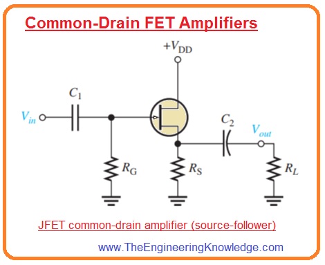
- The common drain junction field effect transistor amplifier is such an amplifier in which input is given to the gate and output is taken out from the source to make drain terminal common for both gate and source.
- As drain is common so there is no need of drain resistance. In below figure you can see the common drain JFET amplifier configuration.
- The common drain configuration is also known as source follower.
- In this circuitry, self-biasing is used. The input voltage is given to the gate with the use of a bypass capacitor denoted as C1 and output is coupled with the load resistance through capacitor C2.
Common-Drain FET Voltage Gain
- Like another amplifier for this amplifier configuration, the voltage gain is Av=Vout/Vin.
- For source follower configuration Vout is
IdRs and Vin is Vgs +IdRs it shown in the below figure.
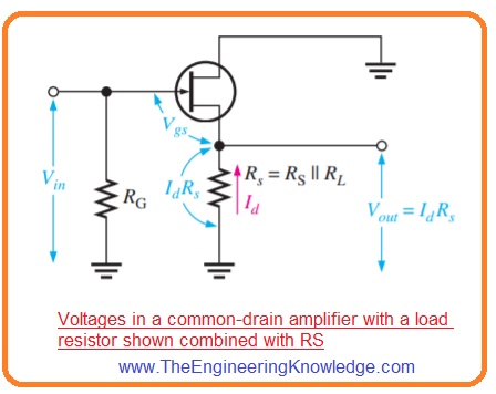
- So gate to source voltage gain will be IdRs/(Vgs +IdRs).
- Putting Id =gmVgs into above equation we have the resultant expression as.
Av=gmVgsRs/(Vgs + gmVgsRs)
- So we have.
Av=gmRs/(1+gmRs)
- Note that the gain value is always less than one. If gmRs>>1 the good approximation is Av=1.
Common-Drain FET Input Resistance
- Since input voltage is given to the gate the input resistance observed by the input signal source is very large like common source amplifier.
- The gate resistance RG is in parallel with the input resistance observing at the gate the total input resistance will be.
Rin=RGΙΙRIN(gate)
- Here RIN(gate) = VGS/IGSS.
So friends that is a detailed post about Common-Drain FET Amplifiers if you have any queries ask in the comments. Thanks for reading. Have a good day.
What is Common Drain Amplifier

- The common drain amplifier also called source follower or voltage follower is amplifier circuitry. It is used in analog circuits for providing high input impedance and less value of output impedance. The input signal is given at the gate terminal and the output is get from the drain pin.
- The main feature of a common drain amplifier is its ability to provide a unity value of voltage gain, which means that output volts follow input voltages. So it is called a voltage follower. The output volts is equal to input vols but with some voltage losses due to the internal resistance of FET
- The input of the common drain amplifier is high which means it does not draw a high current from the input supply. it makes it best to connect where high-impedance signal sources without high loads.
- With that, this amplifier comes with less output impedance, so loads impedance loads can be connected. It offers high current output to load without voltage loss.
- The value gain of a common drain amplifier is about one. It means that the output signal is the same as to input signal in amplitude but has a 180-degree phase difference
- its input is high since the gate terminal of FET work as a voltage controller resistor. Output impedance is low since the source terminal of FET is attached to the ground
- The common drain amplifier is a non-inverting amplifier. its output is 180 degrees from the input signal
Applications of common drain amplifiers:
- Buffering sensitive inputs
- Driving low-impedance loads
- Converting impedances
- Signal conditioning
- Voltage stabilization
FAQs
- What is a common drain amplifier?
- it is also called a stabilizer and is mostly used for constant voltage supplies. The transistor works as an input source is output and the drain is common to the input and output so it is called a common drain amplifier. It is also called a source follower.
- What is the common drain amplifier of a MOSFET?
A MOSFET common drain amplifier uses a MOSFET as the active device. It is like the common drain amplifier that uses a JFET, but the MOSFET comes with a higher input impedance and a low value of output impedance.
- What is the main application of a common drain amplifier?
The common drain can ability to provide high input impedance and low output impedance so it used as buffer amplifier
- What is the common drain amplifier similar to?
it is like the common collector-emitter follower
- What is the most common op-amp?
The most commonly used op-amp is the LM741. It is a general-purpose operational amplifier that is used in different projects
- Why common drain is called source follower
The common drain amplifier is known as a source follower since the source voltage is the same value of the input or gate voltage and is in phase
- What is the ideal maximum voltage gain of a common drain amplifier
The voltage gain is unity, also for the high value of current
- What factors influence the voltage gain of a common drain amplifier
The voltage gain of a common drain amplifier is affected by the some factors:
- Input impedance.
- Amplification factor.
- Drain load resistance.
- Dynamic drain resistance.