 Hello, guys welcome to the new post. Here we will cover What is ENIG plating PCB. Full form of ENIG is electroless nickel immersion gold plating that is performed on PCB boards that have a larger number of coppers pads. The component of projects connected to the PCB board gets the current from the board. In ENIG there are 2 layers of the metal coating is done. At the ist layer of copper pads that exist on the PCB board, the Nickle layer is coated after that thin layer of gold plated.
This type of plating is performed at the upper layer of the copper pad since this plating offered conductive behavior in a well way. That also helps to give fine protection from oxidation and other environmental conditions. Either it is expensive but used due to fulfilling the RoHS criteria. There are numerous PCB suppliers that also fulfill the RoHS in their services such as PCBWAY. That is best in all services also offering ENIG plating services with reasonable prices and good quality since they are equipped with professional engineers and machines. For more than ten years they are fulfilling the prototype and fabrication demands of their customers with high-quality boards, fast delivery, and less expensive products. Since it is the best and most featured PCB manufacturer in China they pride themselves to be your best business partners as well as good friends in every aspect of your PCB needs.
PCB is one of the most important components of any electrical and electronic equipment. PCB quality determines the quality of all these devices. Modern technology makes it possible to increase the miniaturization of composite circuits, higher packaging density, and smaller building sizes, which is why higher demands on PCBs arise.

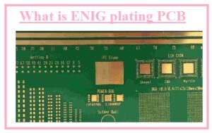
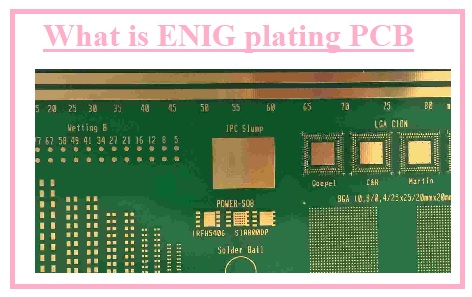
Introduction to ENIG plating PCB
- The most commonly used PCB plating is ENIG. At the bare PCB board, the coating application is called PCB surface finishing.
- The use of ENIG and other types of coating such as HASLis to save the board from external harsh conditions such as corrosion
- ENIG is plated on the pads of coppers existing on the board surface which helps to fight external conditions not favorable for the board.
- First of all copper layers are plated with nickel then the gold layer. The use of ENIG helps to board get an easy soldering process and avoid resistance and plane surface.
- Due to the complicated nature and high cost also used since fulfilling the RoHS.
- ENIG consists of two metal layers first is Nickle on the copper that helps to connect the components.
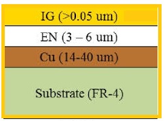
- Another is a gold layer that reduces the connection with other parts. The value of the Nickle layer is four to seven micrometers and gold thickness lies 0.05 to 0.23 micrometers.
- The temperature needed for ENIG is eighty centigrade
Advantages of ENIG Plating PCB
- Some main advantages of ENIG plating are discussed here
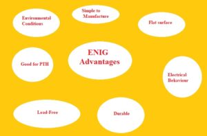
Simple to Manufacture
- Its creation process is simple and easy. Numerous PCB board designers used this plating process for the creation of boards.
Flat surface
- This plating comprises two layers having a metal coating of nickel that protects the surface and easy to connect components.
- This plating fulfills the needs of flat surfaces like BGAs.
Resist to Environmental Conditions
- Every PCB manufacturer prefers to use such a board that resists to oxidation this plating gives this feature. But other surface finishing lack this feature.
- For protection from the oxidation gold layers with nickel is employed on the board.
Fine Electrical Behaviour
- This plating also offered a good electrical operation to board than other plating techniques these parameters also covered with others such as the connection of wires, and finishing design.
A large value of temperature resistance
- The board used in instruments used in medical and military purpose bear the larger value of temperature conditions.
- ENIG finish board comes with these features to handle high-temperature conditions.
Durable
- The finishing used on the board defines the operating life of the board. ENIG plating helps the board to work for twelve months or more. So it is preferred for different project creations.
Lead-Free
- The use of lead inboard can be harmful for health and cause different diseases such as kidney, heart, etc.
- But ENIG plating comes with lead-free features and reduces the cause of harmful diseases due to the board.
Good for PTH
- It is considered as best finishing for PTH. That has wires coming out from the different parts of a breadboard.
Disadvantages of ENIG Plating
- With the same benefits of this plating also has some disadvantages that are described here
Expensive
- As it is considered s fine option for different boards but it is an expensive technique. Some customers used other plating techniques due to larger costs but also used in different projects.
Repairing is difficult
- As this plating is done through the use of machines so engineers face difficulty making again the board if damaged.
- In some case, damage is such that cannot be repaired again and users have to get a new board.
Complex Manufacturing
- Its other drawback is that its manufacturing process is difficult. Other types of plating offered a less complex process than he ENIG.
- Since it was created with the use of machines if machines are not configured accurately then cause serious problems during construction
Black pad of ENIG in PCB
During the permutation of the ENIG technique if there is a high value of oxidation reaction is existing on the nickel surface metal nickel can be transformed into nickel ions then larger size gold atoms get deposited in the shape of coarse and disturbed configuration that indicates that gold layer can completely cover the nickel layer. As a result nickel layer is exposed to air then nickel rust is created under a layer of gold. This nickel rust causes failure of soldering. Therefore other surface finish
In the permutation reaction of the ENIG process, if the nickel surface gets an excessive oxidation reaction, the metal nickel might convert into nickel ions, while the larger gold atoms (radius 144 pm) irregularly deposit to form a coarse and loose arrangement, which means the gold layer might fail to completely cover the nickel layer, allowing the nickel layer to contact with the air, which will finally create nickel rust under the gold layer. This kind of nickel rust will cause soldering failure. This problem called black pad that was solved through the use of ENEPIG which is another type of finish but it is costly that is now just considered for SCP, BGA, or HDI boards
As there is no chance of ENIG finishing to rework the best option is to black pad is a precaution. That is maintain strict control over the nickel bath, that is nickel to gold exchange must be under controlled conditions. The best point is to monitor the pH level of the nickel bath since in this way we can monitor the quantity of excessive phosphorus that is the main cause of the black pad of nickel produced by the nickel dissolution.
ENIG Plating PCB Process
- Preparation of Substrate: The PCB substrate, normally created with fiberglass-reinforced epoxy resin (FR-4), is detailed cleaned and chemically treated to eliminate any oxidation, contaminants, or residues that can affect the plating process.
- Activation: The cleaned PCB board is then treated with a solution having a palladium-based activator. This activator promotes the adhesion of the subsequent nickel layer to the surface of the board. It makes nucleation sites for the nickel to deposit.
- Electroless Nickel Deposition: In this phase, the PCB board is immersed in an electroless nickel bath. The bath comes with a solution of nickel ions, minimizer agents, stabilizers, and pH adjusters. The activated PCB board surface catalyzes the minimizing of nickel ions, leading to the deposition of a thin layer of nickel on the surface. This nickel layer offers a barrier against oxidation and enhances the adhesion of the final gold layer.
- Immersion Gold Deposition: When the electroless nickel layer is deposited, the PCB board is immersed in a solution having gold ions. The nickel layer catalyzes the displacement reaction, causing gold ions to deposit on the nickel surface. The immersion gold layer offers a protective and solderable surface finish for the board.
- Rinsing and Drying: The PCB is completely rinsed with deionized water to eliminate any residual chemicals from the plating process. So, the PCB is dried to avoid water spots or contamination.
- Inspection and Quality Control: The ENIG-plated PCB board undergoes thorough visual and quality inspections to make sure uniformity of plating, absence of defects, and adherence to industry standards.
Faqs
- What is ENIG plating?
ENIG full form is electroless nickel immersion gold. It is a surface finish for printed circuit boards that is characterized by its high solderability, corrosion resistance, and gold content. ENIG is a good option for boards that need high performance and reliability, like as those used in telecommunications, medical devices, and aerospace applications.
- Why is nickel used in ENIG?
Nickel is used in ENIG because it offers different benefits
- Corrosion resistance: Nickel is a very corrosion-resistant metal, which helps to protect the board from damage in conditions and environments.
- Solderability: Nickel has good solderability, which makes it easy to make reliable solder joints.
- EMI shielding: Nickel can help to protect the board from electromagnetic interference (EMI).
- How thick is ENIG plating on PCB?
The thickness of ENIG plating on the board normally has from 0.05 to 0.23 micrometers for the gold layer and 2.5 to 5.0 micrometers for the nickel layer. The exact thickness will change based on certain applications and needs
- What are the advantages of ENIG plating?
ENIG plating provides different advantages than surface finishes for PCBs, like
- High solderability: ENIG has good solderability, which makes it easy to make reliable solder joints.
- Corrosion resistance: it is very corrosion-resistant, which protects the PCB board from damage in harsh conditions
- EMI shielding: it helps to protect PCBs from electromagnetic interference (EMI).
- Gold content: It has a high gold content, which makes it more resistant to oxidation and corrosion than other surface finishes.
- Smooth surface: ENIG has a smooth surface, which makes them best for applications where fine traces are needed
- What are the disadvantages of ENIG plating?
ENIG plating has some benefits, like
- Cost: ENIG is costly than other surface finishes, like HASL.
- Process complexity: ENIG is a more complicated process to apply than other surface finishes, which can cause higher costs and longer lead times.
- Environmental impact: ENIG can have negative environmental effects, due to the use of hazardous chemicals in the plating process.
- What are the applications of ENIG plating?
ENIG plating is a good option for PCBs that need high performance and reliability, like
- Telecommunications
- Medical devices
- Aerospace
- Defense
- Industrial automation
- Consumer electronics
- What are the alternatives to ENIG plating?
Some alternatives to ENIG plating are
- HASL (hot air solder leveling)
- OSP (organic solderability preservative)
- Immersion silver
- How do I choose the right surface finish for my PCB?
The best surface finishes for PCB are based on different factors, like application, the environment, cost, and lead time. If you are making sure of which surface finish is correct for you, you must discuss it with a PCB manufacturer.
- What is the lifespan of ENIG plating?
The operating life of ENIG plating will changes based on the application and the conditions In general, ENIG plating can work for many years, even in different environments.
- How do I maintain ENIG plating on my PCB?
ENIG plating is relatively easy to maintain. You must avoid exposing your PCB board to harsh chemicals or environments. You must also clean PCB regularly with a mild solvent.
That is all about the ENIG plating PCB. all details has been discussing the ENIG plating PCB. If you have any further query ask inc comments. thanks for reading have a good day.