With the advancement of technology and equipment, small and thin form factors are being introduced in electronic tools, so small surface mount technologies are now becoming a common part of PCB boards. PCB boards come with fine pitch, larger SMT components, and medium-sized components. For making these boards, a step stencil is preferred. Here we will cover the detailed features of step stencils and learn how to get this service. Let’s get started.
What is a stencil?
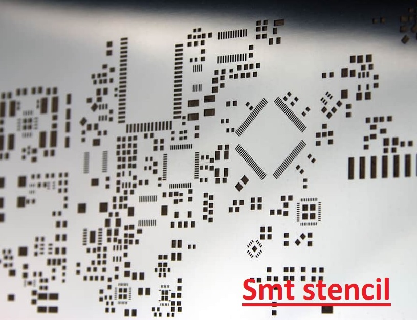
- The connection of SMT components on the circuit board uses deposition of solder paste on board pads. For applications of solder paste, a common method and an accurate module is through the use of a stencil.
- A stencil is basically a thin steel sheet that has holes according to the matching pads on boards.
- When we make the alignment of the stencil on the board, we can allow solder paste to move through the stencil and apply it on the board pads.
- When we separate the stencil from the board, some traces of paste exist on the pads. board having paste move through a pick and place machine, where SMT components are connected on solder paste.
- After component connection, the boards pass through a reflow oven for soldering.
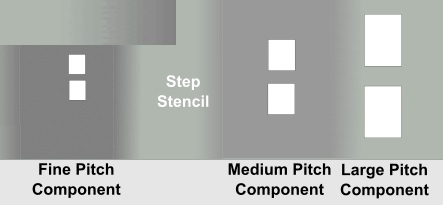
Step Stencil Meaning
- Step stencil SMT is used for easy applications of solder paste volume deposition for small and larger SMT components. Board stencil and solder paste are used for easy connection of larger SMT components.
- thin stencil to use for small SMT components since high solder is not needed
What is Step Stencil?
- Step stencil used for controlling the solder paste amount applied on the board for larger and small SMT components.
- Larger SMT components use high-volume solder paste to get a strong soldering connection, which uses a thick stencil.
- Small SMT components do not need a high solder quantity, and a thin stencil is the best option for using them.
- If your board has small as well as larger SMT components, use a step stencil with thick dimensions at the larger components, and use a thin-dimension stencil for the small components.
Types of Step Stencil
There are two basic types of step stencil: the step-up and the second, the step-down stencil.
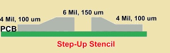
Step-Up Stencil
- If your circuit board comes with many small components connected with a combination of some larger SMT modules, a step stencil is used.
- The stencil used for these boards is made with a steel sheet with a thickness of 0.1 mm, and for larger SMT components, the steel sheet thickness is 0.15 mm.
- Larger thickness makes convex layers that are flat towards the board side.
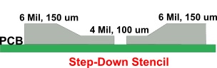
Step-Down Stencil
- If boards have larger-sized components in bulk volume and some SMT components, a step-down stencil is preferred.
- A steel sheet that has a thickness of 0.15 mm is used for small SMT components. The thickness was reduced by 0.1 mm, which makes concave layers with a flat surface towards the board facing.
- Step stencils are used with or without frames; prototype assembly uses frameless step stencils, and framed ones are used for different manufacturing productions.
Best step stencil manufacturing services
- JLCPCB manufacturers are providing services for PCB and PCB-based projects and products at one stop. They are also offering stencil services with the latest and most advanced machines and skilled staff.
- SMT stencil offered at JLCPCB as the earliest service after prototyping, services, and providing reliable SMT assembly all over the world.
- They offer consistent paste, high accuracy, fast turnaround, and full support.
- You can get the first stencil for $0 with a new user coupon!
- They also offer standard laser cuts starting from 7 dollars (380 mm × 280 mm), only $1 with a new user coupon.
- Upgrade to nano-coating or electropolishing for $4.72 more. Fully automated laser cutting services provide fast turnaround in 6 hours.
- Most stencil orders ship within 24 hours of confirmation.
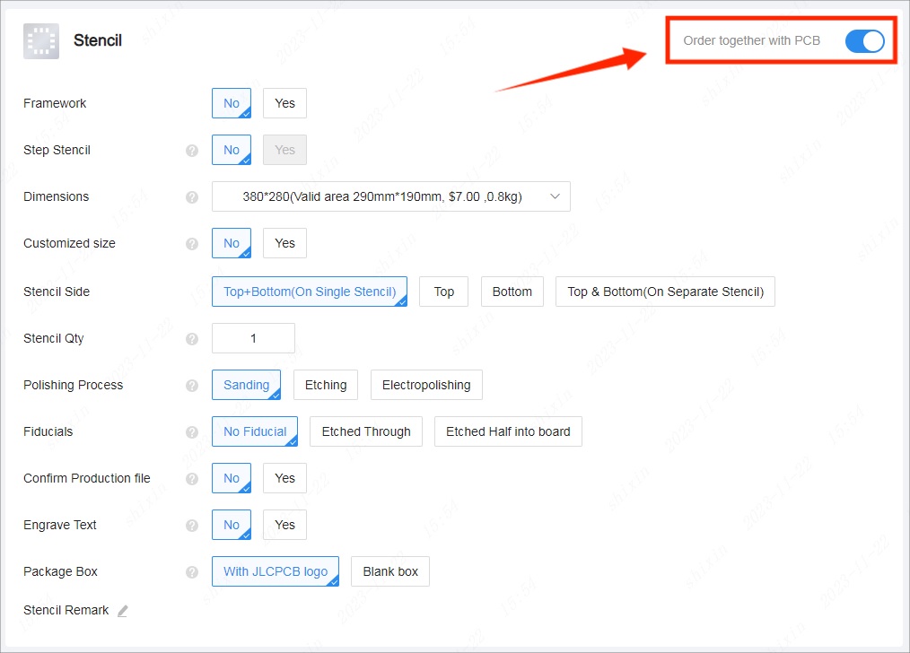
- JLCPCB offers two stencil types. A framed stencil used for automated solder paste printing machines has different standard dimensions.
- A non-framed stencil is used for hand soldering and has a flexible, customizable stencil size and other factors selected according to requirements.
- They are also providing laser-cut stainless steel stencils that are highly accurate and provide disposable features with different conditions.
- Stainless steel stencils are commonly used for balancing project cost and quality. Follow the steps shown in the image to get stencil services.
Manufacturing of Step Stencils
There are three methods used for making step stencils that are explained here.
Photochemical Etching Technology
- It is a basic method that is used for making step stencils. where photographic methods for applications of resist on stencil points where etching does not occur. After that, etchant is used for removing material on the surface to get the required thickness.
Micro-Machining Technology
- In this process, a simple stencil sheet connects with a cooled vacuum plate over the milling machine. For removing even small materials, a CNC milling machine is used to get the required thickness.
- stepped foil connected to the frame and a laser beam used for cutting the required apertures
Laser-Welding Technology:
- Laser welding uses two sheets: a thin sheet with a thick sheet. CNC machines are used for cutting steps on thin and thick sheets.
- A thick foil cut is placed into the cutting part of a thin sheet and connected with a laser weld. For departures, cutting laser beams are used.
Advantages of Step Stencils
The main features of step stencils are as
- It provides optimum solder paste volume control and reduces the different printing processes.
- It has features for the replacement of different stencils.
- It also has solutions for errors like solder shorts, gasketing, and paste smearing.
- It has chances of squeegee steps also relying on the same stencil’s board area,
some problems with stencils
- Stencil thickness and aperture size define applications of solder paste that are deposited on pads.
- For proper soldering of components on the board, solder paste is the main factor. Component soldering is not effective if volume is low.
- High solder can make bridges close to pads if extra paste is applied. For accurate applications of solder paste, the JLCPCB manufacturer uses step stencil SMT with proper thickness and hole size.
- • The board comes with different SMT components that have different footprints that are not good for the stencil; it either comes with a proper aperture or thickness.
- such as ceramic materials easily absorb heat, and solder balls melt at certain reflow temperatures
- while ceramic BGA requires a high melting temperature at the time of soldering. In this condition, a larger volume of solder paste is applied on ceramic BGA pads, requiring a stencil with a thickness of 0.18 and 0.2 mm.
- Very small apertures on the stencil are used for other SMT components, like 0402 chip components and QFPs, which have a 0.5 mm pitch.
- Apertures are good for stencils with a thickness of 0.127 mm since if used for stencils, 0.2 mm thickness causes error.
uses of step-down stencils
- Step-down stencil used where the board comes with one or more fine-pitch components, but mostly the board requires a high solder paste volume.
- 0.006” is the best option, but using a 0.016” pitch QFN causes bad paste releasing and clogged hole sizes.
- Using .004” on the QFN will apply the proper paste volume on the board.
use of step-up stencils
- Step-down stencil prints thin at some points; step-up stencil adds thicker parts that come with standoffs, pin-in-paste, or larger-sized headers for effective solder.
Limitations of Step Stencils
There are some disadvantages of step stencils that are
- It uses a complicated manufacturing process, which requires some extra steps, such as etching and milling, that increase the manufacturing cost.
- It involved some extra steps, so it takes more time for production and increases lead time.
- The manufacturing of the step stencil needed accurate design and planning for PCB design which made it complicated for configuring with component demands.
Step Stencil vs. Standard Stencil
Component sizes
- standard stencil used where components with the same size and solder paste requirements, like designs using 0805 or 0603 passives, are needed. It is good for pitches more than 0.8 mm.
- Step stencil used where if PCB comes with fine-pitch components with larger components such as power modules and connectors.It is used where high-density design is needed.
Board Complexity
- • The standard stencil used for low- to mid-density boards with smooth application is not affected badly.
- Step stencil used where complicated, high-density boards with more accurate control than solder paste volume are needed to prevent defects.
manufacturing volume
- Standard stencil part of low-volume applications with low cost is important, and small errors can be solved manually.
- Step stencil is part of high-volume projects where high first-pass products are important for reducing rework costs.
Budget
- The standard stencil is used for low budgets and designs that do not need the latest stencil features.
- Step stencil used where quality factors are needed with a high budget