 Hello friends, I hope you all are doing great. In today’s tutorial, we will have a look at Troubleshoot Faults in Transistor Bias Circuits. In a biased transistor, circuitry transistor can damage or resistance in bias circuitry can also damage. We will discuss numerous options in this post with the use of voltage divider biasing circuit configuration. Numerous circuitry damaging occurs due to the open resistance, open transistor leads interiorly and junctions or short circuit of junctions.
Frequently, these failures can cause an apparent cutoff or saturation state when voltage is fined at the collector. In today’s post, we will have a detailed look at different faults that occurred in the biasing of a transistor and their related results. So let’s get started with Troubleshoot Faults in Transistor Bias Circuits.
Troubleshooting a Voltage-Divider Biased Transistor
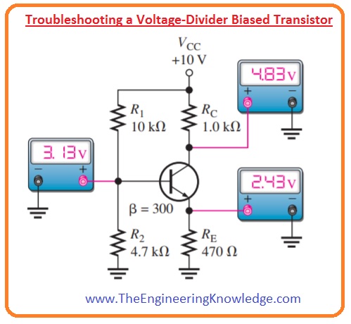
- In below figure circuit of transistor voltage divider bias is shown.
- For a specific value of any component as shown you can get voltage values as denoted when circuitry is working well.
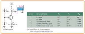
- For such type of biasing circuitry specific types of errors will cause the collector of the transistor to be at VCC when calculated with respect to ground.
- The value of collector voltage is ten volts for every error as shown in the below figure.
- With that value of base and emitter voltage is shown.
Error 1: Resistor R1 Open
- Due to this error bias voltage removes from the base that linking the base terminal with the ground by resistance R2 and transistor goes into the cutoff region since base voltage VB and base current IB is zero.
- As transistor is not conducting as there is no collector current flowing and also there is no voltage loss about the resistance RC.
- This causes the collector voltage to become equal to the ten volts or VCC.
- This makes the collector voltage equal to VCC (10 V).
- As there is no IB or IC is flowing due to that there is no emitter current and emitter voltage is zero.
Error 2: Resistor RE Open
- This error stops IB, IE, and collector current except for a very minor ICBO that can be ignored.
- As the collector current is zero amperes there is no voltage loss about resistance RC so VC = VCC = 10 volts.
- The voltage divider circuitry generates a voltage at the base terminals with respect to ground as given below.
VB =( R2/ R1 + R2)VCC
= (4.7 kΩ/ 14.7 kΩ)10V=3.20volts
- When a voltmeter is attached with the emitter it gives a current path through its large interior impedance that results in forward biasing of base-emitter junction.
- So the emitter voltage is VE = VB – VBE. the amount of forward voltage loss about the base-emitter junction depends on the current.
- CBE is taken as 0.7 volts for the purpose of explanation but it can be less.
- The emitter voltage will be.
VE = VB – VBE = 3.2 V – 0.7 V = 2.5 V
Error 3: Base Internally Open
- The chance of occurrence of an interior fault is larger than the open resistance.
- As The transistor is not conducting collector current is zero ampere and VC=VCC=10 volts.
- To open the RE the voltage divider generates 3.2 volts at the exterior base joint.
- The value of the voltage at exterior emitter connection is zero volts as there is no current flowing through emitter resistance RE and there is no voltage loss.
Error 4: Emitter exteriorly Open
- Again we say transistor is not conducting due to that collector current is zero ampere and VC=VCC=10 volts.
- To open the emitter resistance RE and the interior open base the voltage divider generates 3.2 volts.
- The voltage at the exterior emitter is zero volts since this point is open and linked to the ground with the emitter resistance RE.
- You can note that error three and four showing same symptoms.
Error 5:Collector Interiorly Open
- As there in transistor internally open there is no collector current flowing due to that VC=VCC=10 volts.
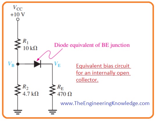
- In this condition the voltage divide is linked with load resistance RE through the forward bias base emitter junction. It shown in below.
- The base emitter voltages are find here.
VB= [(R2││RE)/ (R1+R2││RE)]VCC+0.7
=(427Ω/10.427kΩ) 10 V + 0.7 V = 0.41 V + 0.7 V = 1.11 V
VE =VB-VBE = 1.11V-0.7 V = 0.41 V
Error 6: Resistor RC Open
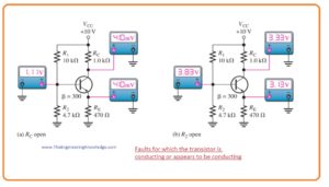
- In this error that is explained in circuit denoted as (a) the collector voltage can lead as to think that the transistor is in saturation state, but in real it is not conducting.
- Apparently, if RC is open correct, there is no flow of IC.
- In this condition, the resultant bias circuitry is similar to error number five as shown in below figure.
- So VB is equal to 1.11 volts and as the base-emitter junction is forward biased.
VE = VB-VBE=1.11V-0.7V= 0.41V
- When a voltmeter is attached to the collector for measurement of VC a current path is delivering though the interior impedance of meter and base-collector junctions in forward bias through the VB.
- So
VC= VB -VBC=1.11V – 0.7V = 0.41V
- The forward loss about the interior transistor junction dependent on the current.
- We take 0.7 volts for an explanation but the forward loss can be less.
Error 7: Resistor R2 Open
- When the resistance R2 is open as shown in the above circuit denoted as (b) the current and voltage of base increases from the normal calculations since the voltage divider is now created by R1 and RIN(BASE).
- In this condition the value of base voltage is found by the emitter voltage VB = VE + VBE.
- Ist , confirm either the transistor is in saturation condition or not.
IC(sat)= VCC -VCE(sat)/ RC + RE
=9.8V/1.47 kΩ=6.67 mA
IB(sat)= IC(sat)/ βDC
=6.67 mA/300=22.2 uA
- By supposing that transistor is in saturation state the extreme base current can be calculated.
IE(sat)= 6.67 mA
VE = IE(sat)RE = 3.13V
VB = VE+VBE = 3.83V
RIN(BASE=BDCVB/IE=(300)(3.83 V)/6.67mA=172 kΩ
IB=VCC/R1 + RIN(BASE)
=10 V/182 kΩ= 54.9 mA
- As this amount of IB is sufficient to generate saturation so transistor will surely go inot saturation region.
So VE, VB and VC will be given as.
VE = 3.13V
VB = 3.83V
VC = VCC – IC(sat)RC
= 10 V – (6.67 mA)(1.0 kΩ) = 3.33 V
So, friends, it is a detailed post about the Troubleshoot Faults in Transistor Bias Circuits if you have any query ask in comments. See you in the next post have a good day.


Transistor circuits for battery discharging…