 Hello friends, I hope you all are doing great. In today’s tutorial, we will have a look at Transistor Biasing Method. In electronic devices and projects, transistors are very commonly used like amplifier and switch. For proper working transistors in this circuits specific amount of current and voltage is needed. The methods to provides these conditions to transistor circuitry called transistor biasing.
In the previous tutorial, we discuss the most commonly used biasing method voltage divider bias of transistor. In today’s post, we will have a detailed look at some other related biasing methods of a transistor and their related parameters in detail. So let’s get started with Transistor Biasing Method.
Transistor Biasing Method
Emitter Bias
- Emitter biasing gives good bias stability in spite of variation in temperature or β.
- It consists of both a negative and positive voltage source.
- To get an estimation of the main dc parameters in an emitter-biased circuitry, analyzation is very easy
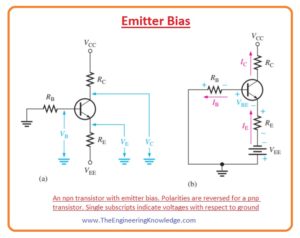
- In NPN circuitry shown in below figure. In this circuit small value of base current decreases the base voltage less than the ground.
- The emitter voltage is 1 diode power loss less than this.
- The combination of less loss across RB and VBE causes emitter to be at almost minus one volts.
- The value of emitter current will be.
IE=(-VEE – 1V)/RE
- In this equation VEE is taken as negative.
- We can use this factor that IC=IE for measurement of collector current.
VC = VCC – ICRC
- The estimate that VE=-1V is valuable for troubleshooting since you would not prerequisite to do any complete measurements.
- The estimate in which VE=-1V and the neglecting of βDC will not be good for designing or complete analysis.
- In this condition, KVL can use to find a detailed equation for IE.
- KVL is used on the base-emitter of circuitry denoted as a. that reconstruct in figure denoted as b for analysis. It provides this below equation.
VEE + VRB + VBE + VRE = 0
- By applying ohm law we have.
VEE + IBRB + VBE + IERE = 0
- By putting IB= IE/βDC and taking transpose of VEE.
(IE/βDC)RB+IERE + VBE = -VEE
- Now we have.
IE=-VEE -VBE/(RE +RB/βDC)
- The voltages taken with respect to ground are taken as single subscript.
- The emitter voltage with respect to ground will be.
VE = VEE + IERE
- The value of the base voltage with the ground will be.
VB = VE + VBE
- The collector voltage with respect to ground will be.
VC = VCC – ICRC
Base Bias
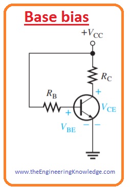
- This type of biasing is mostly used in switching circuits. In below figure base biasing of a transistor is shown.
- If we do an analysis of this circuitry for the linear region it indicates that it depends on the on starting with KVL about the base circuit.
VCC – VRB – VBE = 0
- By putting IBRB for VRB we will have.
VCC – IBRB – VBE = 0
- By solving it for base current.
IB=VCC – VBE/RB
- By applying KVL to given below circuit we have this resultant equation.
VCC – ICRC – VCE = 0
- Solution for VCE.
VCE =VCC -ICRC
- Putting the expression for IB into the equation IC = βDCIB the result will be.
IC=BDC(VCC -VBE/RB)—-(A)
Q-Point Stability of Base Bias
- The equation (A) shows that IC depends on the βDC.
- The drawback of this is that changing in βDC changes IC that also varies the VCE.
- Due to that Q point varies of a transistor.
- It causes the base bias circuitry enormously beta-dependent and unpredictable.
- As we know that βDC varies with the variation in temperature and IC.
- In results, there is a difference in βDC for different transistors due variation in the manufacturing process.
- Due to this cause base biasing is very less used in linear circuits.
Emitter-Feedback Bias
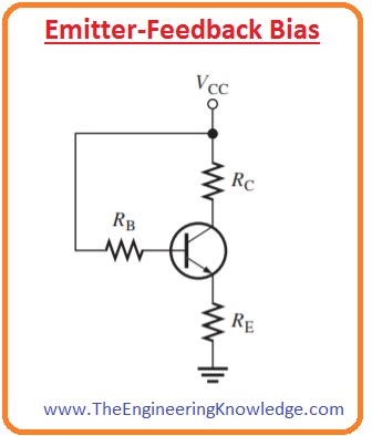
- If emitter resistance is connected in base biasing circuitry the resultant circuitry will be emitter feedback bias as shown below.
- The main function is to make base bias probable with negative feedback, which reduces any variation in IC with an opposite change in IB.
- If IC increases the emitter voltage increases that result in an increment in base voltage since VB =VE + VBE.
- This increment in VB decreases voltage about the RB resistance that decreases IB and IC increases continuously.
- The same results come if IC decreases. It is good for linear circuitry than base biasing, it also depends on the βDC.
- For measurements of IE KVL is applied about base circuitry.
-VCC + IBRB + VBE + IERE = 0
- By putting IE/βDC for base current we can observe that emitter current still depends on βDC.
IE=VCC-VBE/(RE+RB/βDC)
Collector-Feedback Bias
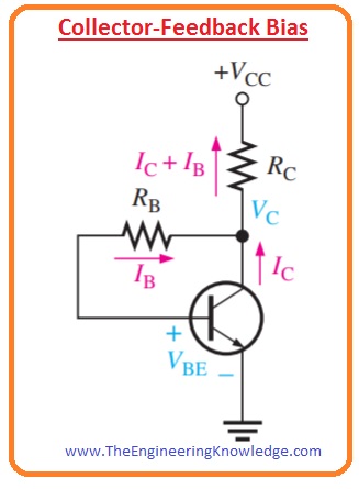
- In below figure base resistance RB is attached with the collector than the VCC as we have discussed it in base bias.
- The collector voltage delivering bias to the base-emitter junction.
- The negative feedback makes the offsetting the effect that stable the Q point.
- If collector current increases, there will be large voltage loss about resistance RC due to that VC decreases.
- When VC reduces the voltage across resistance RB also decreases that reduces the base current.
- Due to decrement in base current reduces the collector current that reduces voltage loss about RC and that offsets decrement in VC.
Analysis of Collector-Feedback Bias Circuit
- By using ohm law base current equation can be written as.
IB=VC – VBE/(RB)—-(b)
- Let suppose that IC is greater than IB. The collector voltage will be.
VC =VCC – ICRC
IB=IC/βDC
- By putting value of VC in the equation (b).
IC/βDC=VCC – ICRC – VBE/RB
β
- It can also write as.
ICRB/βDC+ ICRC = VCC – VBE
- It can also solve for collector current.
IC(RC+RB/bDC)= VCC – VBE
IC=VCC-VBE/(RC-RB/βDC)—-(d)
As emitter is connected with the ground VCE=VC.
VCE=VCC-ICRC
Q-Point Stability Over Temperature
- Equation (d)indicates that IC depends on the βDC and VBE. This dependence can be decreased by creating RC>> RB/βDC and VCC>>VBE.
- The main factor of collector feedback bias is that it basically removes the dependency even if the specified settings are encountered.
- As you have known βDC changes in direct relation with temperature and VBE changes in inverse relation.
- The increment of βDC increases the collector current.
- The decrement in CBE also decreases the base current that decreases collector current.
- As collector current increases the voltage loss about the RC also increases.
- That decreases collector voltage and so the voltage about RB reduces the base current and offsetting the attempt to increase in collector current and decrease the VC.
- The consequence is that the collector-feedback circuit sustains a relatively stable Q-point. The reverse act happens when temperature reductions.
So, friends, it is a detailed post about Transistor Biasing Method if you have any questions about Transistor Biasing Method ask in comments. Thanks for reading.


