 Hello, readers welcome to the new tutorial. In this post, we will discuss Top PCB Testing Methods and Features. PCB is the very basic portion of every electronic module created since its structure is operational and design is such that must workable for a long time and duration on the basis of material and constructed desing. To make it in proper working its testing has become very necessary from small size projects to high-level complicated design.
There are many faults created in this board according to applications such as damaging of design, stress due to thermal application process and some other components damaging. to find out the faults occurring in the board there is many testing techniques are employed. Here we will also cover some details related to the best PCB supplier and PCB testing service providers that is PCBWAY are taking some serious measures and high-level boards to their users with good quality and demands.
Now testing of PCB assembly boards is considered the very crucial portion of any constructed procedure and project. To fulfill this task several testing tools and techniques are used that are discussed here with detail. So let get started.
Top PCB Testing Methods
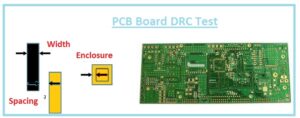
PCB Board DRC Testing
- PCB DRC stands for design rule check and very commonly used at industrial level is the techniques that used to find out the alll applied statistics at the layout of boards are existing and with that production, material fulfills the required features by the constructors.

- To check out these features there is the usage of different tools and software such s CAM software is normally used for DRC.
- PCBWAY technical team before sending the product to users ensure to make sure that all dimensions and parameters of boards are completed.
- Dimension of traces how much distance is created amongst boards pads and traces point and also accomplished that there is through-hole spacing in the desired range.
- After making a detailed overview of the board PCBWAY finalized that there is no fault product is sent to users.
PCB Probe Testing
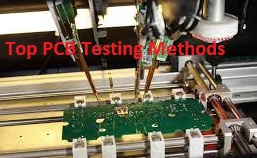
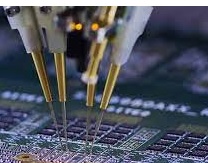
- It is also called the flying needle test used to find the damaging of any conductive path on the board. It is a very less expensive process,
- It can be performed with no use of power. Mian features to perform this test are finding any short circuits, diode damaging, open circuits, capacitors operation in fault, and resistive component damaging.
- At PCBWAY there is the application of automatic optical alignment techniques having modern level probes to find out faults occurs at the board.
- High-level imaging capturing tools and software are used and defected portion is shown on the screen.
Automated Optical Inspection (AOI)
- At the start of construction and finding eh fault occurrence AOI testing is considered as the best test to make sure there is no fault on the board.
- To perform this test there is screenshots and photos of the project’s board is taken and these pictures are then compared to the layout of our board through which we are going to make it.
- This process makes sure that our layout is constructed according to the required design and rules.
- It is considered best for such projects fault detection where there is complication relies in the circuits and detection of fault is difficult to process.
- Their usage of cameras were used for finding the errors existing in the board. It is considered a less expensive test to find out the fault occurrence in multi-layer PCB boards
PCB AUTOMATED X-RAY INSPECTION(AXI)
- Due to being used for the detection of faults occurring in the board, AXI is considered as new and best method.
- X-Ray has features to move to the board for taking the two-dimensional and three-dimensional results of the board.
- Through this process non-accessible points of the board such as BGA and inside existing pads detection become easy.
- This technique is also helpful in finding out the voids of the soldering point. If it is employed with manufacturing procedure this technique is considered as fine to check the fault existing at starting.
- PCBWAY also uses 2D and 3D AXI techniques to accomplish the user’s desires about projects.
PCB Functional Testing
- After completion of the construction of the board, there is full and final testing done that is functional or FCT testing..
- It makes sure that all aspects and parameters are fulfilled in the board..
- According to the design and structure of the board, testing nature depends on means whether it will perform in a simple or complicated way.
- Due to flexible natures, this test is sometimes used as a replacement of another PCB test.
- This category of PCB board test pretends the definite functioning setting and so can be straighter than other testing approaches. Though it might be more problematic to determine the basis of any faults and contrasting burn-in testing, functional testing will not clasp boards that damage at the inial of project creation
PCB Underwriters Laboratories (UL) Certification
- PCBWay creates entirely its PCB boards by UL796 rendering to ZPMV2. Other ways a UL mark represents a manufactured goods standard and protection. A UL spot on any artifact is universally acknowledged and tells any project having it fulfilling all desired apartments.
- Beforehand choosing for any PCB testing approaches, PCBWay guarantees that all the ingredients in the construction and analysis of PCB boards should be according to RoHS compliance. PCBWay promises not ever use a component that causes hazard results for nearly area environment. So lead-free surface finishing is used on their board.
That is all about the Top PCB Testing Methods and Features. I have explained here commonly used PCB testing methods and their features. If you have any further query ask in the comments. Thanks for reading have a good day. see you in next post.
.jpg)


