

 Hello, friends, I hope all of you are enjoying your life. In today’s tutorial, I am going to explain Single Sided PCB Board. PCB stands for printed circuit board it also known as printed wiring board. When it was not common to use circuit construction was a very difficult and time-consuming process also costly, because it was done manually. Manually constructed circuits also had less working life and insulation of these circuits was also difficult. After the availability of integrated circuits and different semiconductor materials circuit compositions become easy and the printed circuit board also developed with time.
This circuit board made the construction of circuits too easy, cost-effective, and increases reliability. Now on this board, we can easily make our circuits and projects easily. Almost all electronic devices are manufactured on this board like mobile phones, calculators, and computers. There are numerous types of PCB according to construction and use like single-sided, double-sided PCB, rigid PCB, etc. In today’s post, we will have a look at single-sided PCB its manufacturing, working, uses, and some other related parameters. So let’s get started with what is Single Sided PCB Board.
Introduction to Single-Sided PCB Board
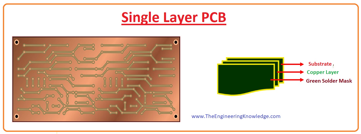
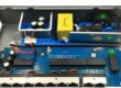
- The single-sided printed circuit board is the basic category of a circuit board on this board only one side is used for the production of different circuits and there is only one side that has conductive parts for the construction of circuits.
- Due to simple construction, its price is also very less, and the best option for new engineering students and project constructors to use it.
- this category of circuit board was first invented in 1950 but due to its simple design and easy use, it is still used in different electrical and electronic projects.
- In 1956 when some engineers of Japan start to work on this PCB this was the time it gets boasted in electronic industries.
- The manufacturing of this board is very easy it consists of copper at one side with the substrate over copper coating for protection of the board solder mask is rapped.
Construction of Single Sided PCB Board
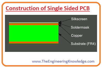
- Due to its simple design, its manufacturing process is very easy, cost-effective and less time-consuming the substrate substance of this board comprises fiberglass to increase the strength of the board.
- On this substrate material, different paths for current flow and components assembly is manufactured with copper, use of copper is due to its best conductive power and less cost.
- The length and diameter of copper paths rely on the manufacturing of the circuit and users demand it measured in ounces per square foot.
- Over the copper conductive path, a layer of solder mask is coated this layer provides safety to copper paths from corrosion due to oxidation and moisture in the environment.
- On both of these two copper and solder masks, there is and third silkscreen layer that is employed for the drawing of different components symbols, and characters, it makes sure users place components at the proper place and with the right connection.
Difference between Single Layer PCB and Double Layer PCB
- These are some main differences between the single-sided printed circuit board and the double-sided circuit board.
Single-Sided PCB Board
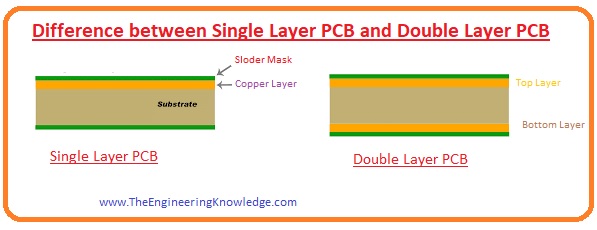
- This circuit board uses only one side for manufacturing o circuits and on another side different conductive paths are manufactured.
- On this board, there is only a single layer of conductive substance, the common use conductor is copper.
- There are three main layers are assembled on this board first one conductor material, the second one is a solder mask that provides protection to the board from outer environment conditions and the third one is silkscreen.
Double-sided PCB
- In a single-sided PCB board, there is one side is used for the production of circuits but in double-sided boards, both sides are used for the manufacturing of circuits.
- This PCB has conductive paths on both sides having copper, solder mask, and silkscreen.
Single Layer PCB vs Double Layer PCB
| Feature | Single-Layer PCB | Double-Layer PCB |
|---|---|---|
| Layer Count | 1 | 2 |
| Copper Conductors | Only on one side | Both sides |
| Component Density | Lower | Higher |
| Trace Routing | Limited | More flexible |
| Manufacturing Cost | Lower | Higher |
| PCB Size | Larger | Smaller |
| Complexity | Simple | Moderate |
| Signal Integrity | Less robust | More robust |
| EMI/EMC Performance | Weaker | Stronger |
| Soldering | Easier | More challenging |
| Power and Ground Planes | Not feasible | Possible, providing better power delivery |
| Design Flexibility | Limited | More options available |
| Noise Susceptibility | More prone to noise interference | Reduced susceptibility to noise |
| Component Placement | Limited space for components | More space for components |
| Cost of Prototyping | Lower | Higher |
| Board Size | Larger size due to limited space | Smaller size due to component stacking |
| Assembly Time | Faster assembly process | Longer assembly process |
| Signal Crosstalk | More significant risk of crosstalk | Reduced risk of crosstalk |
| Layer-to-Layer Coupling | Not applicable | Potential coupling between layers |
| Layer-to-Layer Shorting | Not applicable | Risk of shorting between layers |
Single-sided PCB vs Multilayer PCB
| Feature | Single-Sided PCB | Multilayer PCB |
|---|---|---|
| Layer Count | 1 | More than 2 |
| Copper Conductors | Only on one side | Both sides and internal layers |
| Component Density | Lower | Higher |
| Trace Routing | Limited | More flexible |
| Manufacturing Cost | Lower | Higher |
| PCB Size | Larger | Smaller |
| Complexity | Simple | Moderate to high |
| Signal Integrity | Less robust | More robust |
| EMI/EMC Performance | Weaker | Stronger |
| Soldering | Easier | More challenging |
| Power and Ground Planes | Not feasible | Possible, provides better power delivery |
| Design Flexibility | Limited | More options available |
| Noise Susceptibility | More prone to noise interference | Reduced susceptibility to noise |
| Component Placement | Limited space for components | More space for components |
| Cost of Prototyping | Lower | Higher |
| Board Size | Larger size due to limited space | Smaller size due to component stacking |
| Assembly Time | Faster assembly process | Longer assembly process |
| Signal Crosstalk | More significant risk of crosstalk | Reduced risk of crosstalk |
| Layer-to-Layer Coupling | Not applicable | Potential coupling between layers |
| Layer-to-Layer Shorting | Not applicable | Risk of shorting between layers |
Single-Sided PCB Board Advantages
These are some important benefits of a single-sided printed circuit board.
Lower Cost:
- As we discussed above that the physical structure of the PCB is simple than other types of PCB and needs less material, time and less practical experience. All these facts make it cost-effective.
Simpler Design
- Its construction and design are so simple that any normal designer can construct it without any special expertise. It always prefers over other PCBs due to its simple design and production in fewer time intervals.
- Most PCB users prefer it due to its simplicity in design and it is the best choice for new users of this board.
High Volume:
- Due to simple design, these circuit boards are manufactured in large numbers, and due to high quantity, their price automatically decreases.
Short Lead Time:
- Another benefit of this board is that it can be manufactured in very less time and in large quantities which makes an instant option for users of PCB.
Single-sided PCB Disadvantage
- Where it has some advantages there are some disadvantages that every user should keep in mind.
Simple Design:
- The simple and easily manufacturing design of single-sided PCB make effective for users but it also has some limitations.
- For such circuits where large numbers of components to be assembled need large space and more connection points that are lack by the board.
- If we construct circuits on this board with a large amount there is a chance of short circuits and can damage or devices if proper insulation is not done.
Slower Speed
- The minimum no of components joining points also disturbs its speed and power. Due to its less operating speed, it is not favorable for such applications where a large no of connections are needed.
Large Size:
- For the addition of a large no of components, there is a need to make its size which also increases its weight and cost too.
Single-Sided PCB Board Pros
- Before the implementation of single-sided PCB, you should also need to study some factors either it is fulfilled the requirements of your projects or not. And you should also note these pros and cons before choosing this category of a printed circuit board.
- Its price should be less.
- Its design should be simples and easy to handle.
- It has a smaller leading time.
Single-Sided PCB Board Cons
- Its design is not suitable for complicated projects so its best for these circuits.
- Its working capacity is also less.
- Its operation speed is also less.
- Due to its large size, it is expensive.
- Due to large components assembled on a single board, its weight is also large.
Applications of Single-Sided PCB Board
- These are some applications of a single-sided printed circuit board.
- Due to less price and easy construction, it is mostly used for different engineering projects.
- As other types of PCB are growing fastly but single-sided PCB importance cannot be denied for simple circuits.
- In our home appliances like coffee makers are constructed by the single-sided circuit board.
- In calculator mobile phones, radios and light-emitting diodes are consist of these boards.
- The solid-state driver also consists of this PCB and different sensors are also constructed with a single-sided PCB board.
Related Posts
- Aluminum PCB (Printed Circuit Board)
- Multilayer PCB (Printed Circuit Board)
- Rigid PCB (Printed Circuit Board)
- Flex PCB (Printed Circuit Board)
- High Frequency PCB (Printed Circuit Board)
- Single Sided PCB (Printed Circuit Board)
- Rigid-Flex PCB (Printed Circuit Board)
- Double sided PCB (Printed Circuit Board)
That is the complete tutorial on the single-sided PCB board I have written each and everything related to this PCB board. If you have any questions about this PCB board ask in comments. Thanks for reading. See you in the next tutorial.


It’s really a nice and useful piece of info. I’m glad that you shared this helpful info with us. Please keep us up to date like this. Thank you for sharing.
I loved as much as you’ll receive carried out right here. The sketch is attractive, your authored subject matter stylish. nonetheless, you command get got an impatience over that you wish be delivering the following. unwell unquestionably come further formerly again as exactly the same nearly a lot often inside case you shield this increase.
Hiya, I’m really glad I’ve found this information. Today bloggers publish only about gossips and internet and this is really irritating. A good blog with exciting content, that is what I need. Thanks for keeping this web-site, I’ll be visiting it. Do you do newsletters? Can not find it.
I appreciate, lead to I found just what I was taking a look for. You’ve ended my 4 day lengthy hunt! God Bless you man. Have a nice day. Bye
I don’t even know how I ended up here, but I thought this post was good. I don’t know who you are but certainly you’re going to a famous blogger if you are not already 😉 Cheers!
Hey there! I could have sworn I’ve been to this site before but after checking through some of the post I realized it’s new to me. Anyhow, I’m definitely delighted I found it and I’ll be bookmarking and checking back frequently!
very nice put up, i certainly love this web site, carry on it
I loved as much as you’ll receive carried out right here. The sketch is tasteful, your authored subject matter stylish. nonetheless, you command get got an edginess over that you wish be delivering the following. unwell unquestionably come further formerly again since exactly the same nearly very often inside case you shield this increase.
My brother suggested I might like this website. He was totally right. This post truly made my day. You cann’t imagine simply how much time I had spent for this information! Thanks!