Hello, readers welcome to the new post. We will discuss 4-layer Ultra-thin 0.25 mm and High Density HDI PCB. Nowadays HDI PCB boards are considered the main part of PCB projects and electronic device circuits. HDI offers numerous benefits over other PCBs which enhance the features of the required design. Through having the accurate design and expert PCB suppliers such as PCBWAY that provide high-quality HDI boards you can enhance the quality and operation performance of your devices.
The PCB board having one twenty to one sixty pins per square inch is called HDI PCB. These boards have features of high-density component placing and versatile routing. Monrovia technology is only used for HDI PCBs. For dense structures micro via, blur via, and blind via are used.
The use of HDI techniques in electronic engineering provides the possibility for engineers to assemble multiple components on both surfaces of a general PCB in some specific requirements.
With the development of via in pad and blind via techniques, they make it easier for engineers to assemble small-sized features over a short distance.
The common application of HDI PCB is in mobile phones, such as devices that have touch display computers laptops, and digital cameras.
HDI boards help to connect the larger number of components on both sides of the ds permitting adding more functions at smaller areas with good features. These boards help to enhance the electrical performance of boards. PCBWAY has introduced new features for 4-layer Ultra-thin 0.25 mm and with High-density HDI boards. Here we will cover the details of these features of PCBWAY.
4-layer Ultra-thin 0.25 mm and High-Density HDI PCB
- With the advancement of technology, the current projects’ design and circuits are now getting smaller and thinner in structures, these features enhance the use of HDI technology and with that also promote the use of ultra-thin and high-density HDI boards. These boards come in smaller structures having a larger quantity of holes with larger dense lines.
- Ultra-thin. As a complex technique, PCB boards come with different features such as ultra-thin, high density also high accuracy
What is HIgh-Density blind holes and Ultra Devices
- The laminate pressing of FR4 resin was used to make the ultra-thin and high-density HDI multilayer plate with a combination of a mi-curing palate and electrolyte copper sheet.
- Some complications involved are laminated pressing of ultra-thin core plate laser drilling and mechanical drilling. There are many issues such as plate deformation, uncontrolled thickness, nd deviation in interlayers that in the manufacturing process
Intro of Products
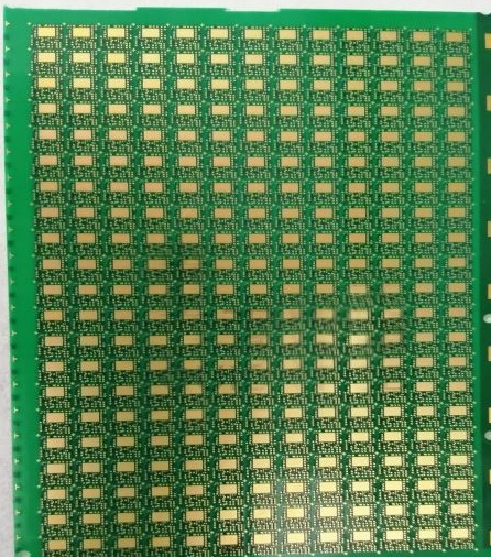
- From PCBWAY you can get 4 layers first order HDI (1+2+!) boards with a thickness value for the finished plate of about 0.25m +/-0.025mm
- The dimension for the mechanical pass is about 0.1 mm282038 holes
- The dimensions for minimum laser hole 0.1 mm with a single size 5 x 5 mm 546 pieces per set
Control Features for HDI PCBs
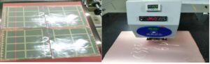
Inner drilling
- The quantity of holes is about 282038 with a core thickness of 0.065 mm in the absence of copper is 0.065mm. When the opening is done copper size is reduced by about seven to nine micrometers. The drilling device used in the internal layer is about 0.1mm for this purpose updated drilling nozzle is applied. To avoid the lance, PCBWAY uses the phenolic pad
- The thickness for pressing is about 0.22mm one piece 106 P layout 4pnl/layer that regulates the lack of glue and shrinkage
Laser Drilling
- The density for the r hole is about larger in size T surface 428241 holes aperture 0.1 mm B surface 917457 outer single 106 PP internal core plate 0.065 mm, copper thickness 18um helps to regulate the laser energy control laser breakdown, and laser hole category.
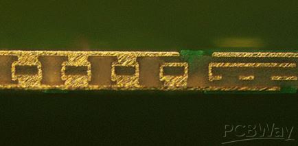
- The thickness of the te is at 0,25mm and the external copper layer dimensions is about 18 micrometers so laser holes are filled through the use of the baffle
- Pad comes in a smaller size so solder mask used is created through the LDI and the surface is covered with the nickel palladium gold processing
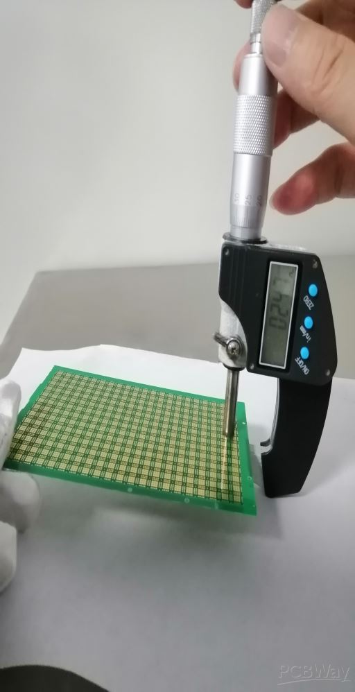
- At last thickness of the boards is measured through the measuring devices
- The final finished plate is about 0.247 mm which is a feature of PCBWAY for HDI boards
Further details for PCBWay 4-layer Ultra-thin 0.25 mm and High-Density HDI PCB can get here
https://www.pcbway.com/blog/News/Congratulations_on_the_Success_of_PCBWay_4_layer_Ultra_thin_0_25_mm_and_High_Den_9291acf1.html
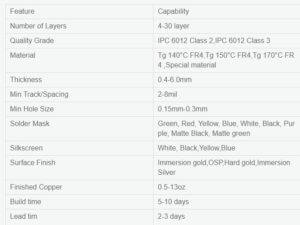
PCBWay HDI PCB manufacturing capabilities
- The features or capabilities provided by the PCBWAY in HDI PCB are in the below featues
That is all about the PCBWay 4-layer Ultra-thin 0.25 mm and High-Density HDI PCB. All details have been explained for PCBWAY HDI boards and ultra-thin 0.25mm thickness, that is helpful for you to make your projects good and precise.


