The PCB board is considered the main component of electronic devices and projects. It is now the main part of small calculators and larger machines used in industries. PCB boards come with different conductive layers for the current flow of components connected to them. For proper electrical conductivity of conductive layers, a coating called PCB plating is performed. PCB plating is the main step involved in the board manufacturing process and helps boards work effectively.
Table of Contents
ToggleIntroduction to PCB Plating
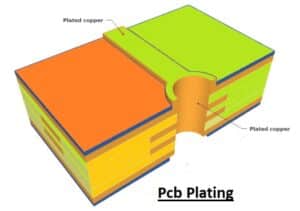
In this process, the conductive layer on the board and pads are coated with a metallic layer to protect the board from corrosion and other environmental factors that help to provide proper conductivity. The process used to apply the layer of metallic layers to the board is called electroplating. Gold is a commonly used metallic layer, and some other metals are nickel, copper, silver, etc. The thickness of metallic layers is based on board structure, design, and project demand.
PCB Plating Types
Electrolytic Plating:
- In this process, a metallic layer is applied to the board with the use of electric current. Electrolytic plating is mostly used for depositing thick copper layers through holes to enhance the conductivity of the board. This process helps to make the copper thickness on the board about 1 oz/ft2 or higher. It offers a uniform and dense metallic layer.
Electroless Plating:
- Electroless plating involves the chemical reaction for the deposition of a metallic layer on board. This process provides uniform plating for non-conductive boards.
Immersion Plating:
- In this process, the PCB is placed in a metallic solution that is applied to the board surface. This process is used where the durability of the board is required.
How to Perform the PCB Plating Process
Board Cleaning
- First of all, the board is cleaned by removing dust particles, oils, etc. For this purpose, cleaning solutions are used.
Etching Process
- Etching is involved in removing additional copper from board surfaces. Unwanted copper was removed with the use of a chemical solution, and just copper traces and pads existed.
Board Pre-dip
- Now the board is dipped in a pre-dip solution that makes the board surface ready for the plating process.
PCB Plating
- In this step, a metallic layer is applied to the board surface. For this purpose, the board is dipped in an electrolytic solution, and power supply terminals are connected to the solution for current flow. As a result, the metallic ions of solutions make a reaction with copper on the board surface, and the metallic layer is deposited.
Post-dip Solution
- In this step, the board is dipped in solutions that make a strong connection between the metallic layer and the board.
Different PCB surface plating finishes

Gold
- Gold is not commonly used, but it is highly conductive. The best feature of gold plating is that it has high oxidation resistance. But due to the high cost, it is not being used.
Tin
- Tin is a low-cost metal as compared to gold, and its easy access makes it common to use for plating boards. Tin plating is also resistant to water and corrosion.
Electroless nickel immersion gold
- ENIG, or electroless nickel immersion gold, is best used for PCB boards due to its lead-free features. In this process, about 150 to 200 microinches of nickel are applied to a copper surface. After that, a gold layer of 3–10 microns was applied to the nickel layer. These finishes save the board from different environmental conditions, but they are costly to process.
Silver plating
- Silver plating comes with some features for boards, such as a flat surface, an easy soldering process, and lead-free coating features. A micron-thick silver layer is applied to the copper layer with the use of an electroless plating process. It is an easy-to-afford process and compatible with the board structure and manufacturing process. But this coating drawback is that it does not handle humidity or temperature variation.
Hot Air Solder Leveling (HASL)
- For HASL, finishing boards are placed in a molten solution of tin or lead. Soluting makes the coating on the copper layers on the board. After that, the board is removed from the solution, and high-pressure hot air is applied to the surface through air knives that flatten the deposited layer and remove extra solder on the board surface. HASL makes proper solder joints and provides effective soldering processes, but HASL coating thickness avoids its use for fine-pitch components.
PCB Plating Techniques
Through-hole plating
- Different techniques are used for creating plating layers on the walls of substrate boreholes. This process is known as hole wall activation for industries, and PCB manufacturing needs many storage tanks that come with the control system.
- Through-hole plating is part of the drilling process. When the drill bit drills through copper layers and substrate, the insulating synthetic resin that is made from the substrate’s base melts due to the heat generated. With that, the molten resin and other drilled fragments were created around holes and adhered to the copper foil’s recently exposed hole walls, which were dangerous for the newly made plating surface. The molting resin forms a hot axis on the substrate hole walls.
- It does not have proper adhesion for some activators and needs a process for removing statin and etching back the chemistry.
Brush Plating/Selective Plating:
- Brush plating is applied to a certain part of the boards. In this method, a limited part is dipped in electrolyte. In this process, rare metals are applied to a selective part of the board. For this process, a chemically reactive anode is used, such as graphite. The anode is covered in cotton sticks or other absorbent materials. It is the best method for applying solutions to certain parts. Normally, this type of plating can be seen on board edge connectors. .
Finger-plated Plating:
- In the finger plating method, also called protruding partial plating, rare metals are applied to edge connectors or board edge joints. The application of rare metals helps boards have high abrasive resistance and less contact resistance.
Reel Linkage Selective Plating:
Different types of pins and contact pins of electronic components like ICs, transistors, and flexible boards are used for selective plating for proper contact resistance and corrosion resistance. A manual process or machine was used for this plating process, which was a high-cost process due to the selection of pins and involved batch welding.
Metallic foil that needs to be flattened and requires proper thickness is die-cut, cleaned, and then used as a continuous plate in different combinations, such as nickel, iridium, button, gold, silver, tin-nickel, copper-nickel, or nickel-lead alloy. In this process, the first of all metallic copper foil components that are to be plated is coated with a resist layer, plated, and applied to specific parts.
PCB Plating Thickness Values
The normal value of PCB plating thickness is about 100 microinches. The value of thickness for OSP and singing silver is about 10 micro inches of a thin layer.
Two reasons define why PCB plating thickness is important.
- First, the IPC 2221A standard defines the minimum value of plating thickness for every IPC product. If there is a need for your product to conform to IPC, then follow standards for plating thickness. So before manufacturing, the board first considered the mining thickness values.
- Another factor is the effect of PCB plating thickness on losses. For low-frequency values, there will be no effect on PCB plating thickness. Losses occur when millimeter-wave frequencies like short-range radar (24 GHz) and higher are used. On these frequency values, copper roughness is the loss factor.
Read also:
- PCB Voltage Regulators: Types and Applications
- PWB vs PCB: Differences and Similarities
- Matte vs Glossy in PCBs
- Lead vs. Lead-Free Solder in PCB Manufacturing – 2024 Ultimate Guide
- What is Rogers Ceramic PCB and How Much Do Those PCBs Cost
Faqs
- There are different plating techniques used; the common ones are solid surfaces covered with metallic sheets and heat and pressure applied to fuse them. Some other plating processes are vapor deposition under vacuum electroplating and sputter deposition.
- PCB plating is an electrochemical process that is deposited on the surface of a board and plated through holes.
- ENIG is a common and famous technique and is used for about 80 percent of PWBs. This finish offers a thin, gold, easy-soldering layer that protects copper traces with a nickel layer between it and copper. ENIG is lead-free, durable, and has a long-lasting finish.
- PCB button plating, also called pad-only plating, defines the manufacturing process used for flex boards. This process involves electroplating copper on board vias and on-board pads that capture vias.
- Coating is used to handle irregularities in the board structure and PCB environment. It offers good dielectric resistance, and proper integration, and protects boards from corrosion, humidity, fungus, and dust particles.
- Commonly used materials for metallic layer manufacturing are copper and aluminum, but stainless steel is also used. Coper has the best operations and electrical features as compared to aluminum but at a high cost.
- The panel-plated layer comes with a thick copper thatn button-plated layer. It affects current-carrying features and voltage losses over conductor length.
- It protects the board from moisture, oxidation, and environmental conditions.
- It helps to reduce the board manufacturing cost and also decreases construction time.
What are the main types of PCB plating techniques for PCB manufacturing?
- Selective plating
- Surface mount technology (SMT) plating
- Through-hole plating