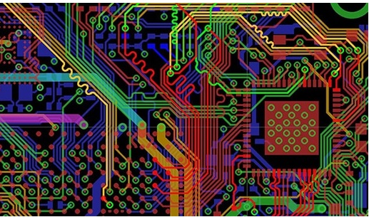
 Hello, readers welcome to the new post. We will discuss PCB Fabrication Process. PCB is considered as the main part of the electronic industry and used in industries. It is an integral part of the computer industry, with that medical devices aviation industry as well used thee, boards. PCB comes with a layer of copper at top of the boards with a different symbolic representation of different components to make the connection of projects.
There are different types of PCB such as single layer, double-layer multiple layers rigid, flex, etc. All these boards are used in different applications since having different features. Today we will cover the details for PCB PCB Manufacturing that will help to get the good PCB for our projects.
Structure of PCB
- For the fabrication of PCB, we must have some understanding of PCB structure.
- There are 4 main parts of PCB.
- Substrate
- Copper Layer
- Solder Mask
- Silkscreen
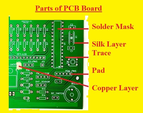
PCB Substrate
- The substrate of PCB is the basic part where all other components reside. It is created through the use of fiberglass also FR4 materials is used. Fiberglass is preferred since has strength and resits to any pressure breakage.
Copper Layers
- Over the substrate copper, layers are placed these layers help to transmit the signal among the connected components.
Solder Mask
- Over the copper layers, there is a layer of solder mask that protect the copper layers to get short circuit with any other parts and get corrode from the environmental conditions.
Silk Screen
- At the upper part of the board, there is silkscreen layers that come with different symbols of components where these components connect to make the circuits. This part of the board also called nomenclature
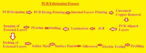
PCB Fabrication Process
- There are many steps involved in manufacturing of that are described here
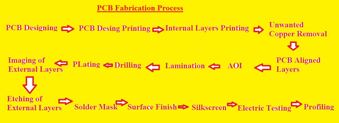
PCB Designing
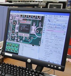
- In first step for PCB Fabrication design of the PCB is created. There are different software used for PCB design. Commonly used software are eagles, OrCAD, KICad Altium Designer, etc. For PCB design there must have an idea and sketch of the circuit in mind. For the creation of PCB layout used for the PCB designer is known as Extended Gerber also called IX274X.
- Extended Gerber is used as output formate. In the Gerber file, all details like layers of boards solder mask required and some other data of boards is stored. When the design is final through Gerber extended then final overview is done to avoid any fault in the design. After that design is sent for PCB Fabrication. When using get but he PCB manufacture another inspection od design is done the called DFM
PCB Desing Printing
- Printing of PCB started when the designer finalize the results of PCB design DFM checking is done by the fabricator. There are certain types of printers called plotters used to make the outs of PCB design. Plotters are used to provide clear results of PCB design
- There are two color layers can see in this film of PCB design.
- Black ink is used for copper traces and circuits while clear ink is used to mention the non-conductive point of PCB for example substrate that is of fiberglass
- External layers of PCB design come with clear ink to denote the copper lines and black ink is used to parts where copper is eliminated.
Internal Layers Printing
- In this PCB Fabrication is started by the PCB manufacturers. The design of PCB is made on the laminated material after that copper is attached to that laminated material. Coper is eliminated to get a clear design of the board. The laminate panel is coved through the photo-sensitive film known as film. This resist helps engineers to make the accurate configuration among the pictures of design and photoresist.
- After the application of resists, resultant products are passed through UV light.UV lights help to harden the photoresist.
- When the board is created cleaned through the use of the alkaline solution to eliminate additional photoresists. After those boards is got dry. When the PCB drying process is completed just leave the resist that is a portion of PCB. Inspection od done by the engineers to check the faults. If there is no faults exist then PCB passes to the next steps
Unwanted Copper Removal
- There is additional copper is existed in the internal layers of the board to move to other steps. A chemical solution is used to remove the extra copper. While required cooper remains covered below the photoresist.. Different boards are having different layers and different amounts of copper so the solution used will be different for each copper removal
PCB Aligned Layers
- When extra copper from each layer is removed it passes through the alignment process. Holes help to align the internal and external layers of the board. An optical punch machine is used for the alignment of layers. This machine presses the pins in the holes to align the layers
AOI or Automated Optical Inspection
- To find the faults and defects there is an optical inspection done. When layers get aligned so difficult to find the faults so an AOI inspection is performed to find the faults according to the Gerber file. After that board passes to the next steps
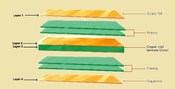
PCB Layers Lamination
- When there are no faults found in the PCB lamination of the board is done. Two steps are involved for PCB layer lamination. The first one is to lay up a step and 2nd one is laminating step
- The external layers comprise of fiberglass sheet, pre-impregnated having epoxy resin called prepreg
- The metallic clamps are used to bond these layers on a certain type of pressing table. Every layer is adjusted at that table through the use of certain pins. For lamination, the prepreg is placed on the table. The substrate is placed on the pre-impregnated resin having a copper layer. Then more sheets of pre-impregnated resin are placed and at last copper, the piece is placed that is known as a press plate.
- After placing the press plate the complete material is pressed. Through mechanical pressing complete stack is pressed using pins.
- Then PCB stack is moved to the laminated press. There is the application of heated plates to use heat and pressure for stacking the layers. The heat from the plates removes the epoxy resing existing in the prepreg and bonds all layers
PCB Drilling
- Now drilling is performed for this process X-RAY machine is used to find the points for drilling. Some sample holes are drilled into the resulting PCB stack to get accurate holes during proper drilling. For drilling computer-guided drill is used to make the correct drilling according to Gerber
PLating of PCB
- The plating process helps to bod all layers of boards through the use of chemicals. Then PCB passes through chemicals. Through this process, micron thick layer of copper is placed on the upper part of the layer, and drilled holes
- When the holes get filled with copper exposed to a fiberglass substrate that helps to make a panel.
Imaging of External Layers
- In step 3 photoresist was applied to the PCB. Now other layers of this resistance will be applied on the board. Now photoresists are applied to the external layers. After photoresist and making the image of external layers the layers plated in the same fashion as the inner layers done
Etching of External Layers
- The tin guard is employed for the protection of copper when etching is done. Through the use of the solution, non-desired copper is removed. Tin helps to protect the required copper used for etching
Application of Solder Mask
- Now apply the solder mask for this first clean board through the use of epoxy solder mask ink. Bals of UV light is applied on the board that passes in the solder mask photo film.
Surface Finish
- To enhance solder features of board gold paled with gold or silver. With that hot air, leveled pads are also used over the board. that results in uniform pads
Silkscreen
- Silkscreen is applied that has different symbols of components where electronic components connect to make the circuits
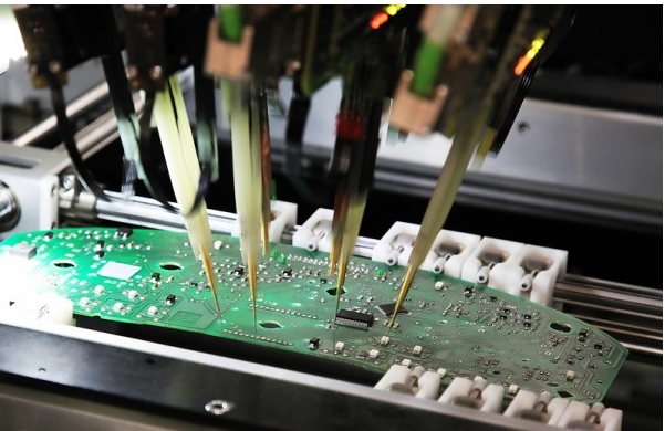
Electric Testing
- Electrical tests are performed to find the accurate operation of the board. Different tests like flying probes are done for this purposes
Profiling
- Here the last step is to cut different boards from the real panel. The technique used for this purpose is a router or V-groove. V grooves help the diagonal parts of the board and routers leave the smaller tabs about the board corners. These two techniques help to get the board accurately from the panel
Read also: