Hello readers welcome to the new tutorial. Here we will discuss PCB Design with EasyEDA . PCB is a very basic part of any electronic project so it needed certain demands and precautions for the creation of it and making its design. There are different ways that are used for the creation of the board here I will tell you basic and simple way through EasyEDA PCB design. After that will tell you how you can get the PCB after making design from JLCPCB which is the best PCB supplier in the world.
PCB Design with EasyEDA & JLCPCB
- To design PCB board through EasyEDA and also I am using it to make the design.
- First of all you have an account on the EasyEDA site for this purpose type EasyEDA in google and visit their site.
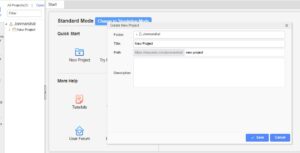
- If you new user of EasyEDA press on the register button shown below

- When you press on the register button new interface will open here put all details and press sign up button then verification email will you get on your email press on it and activate your account.


- Move to EasyEDA site then log to your account after that press on EasyEDA designer tab then new projects tab will seen press on it and write the name of your project then save it.
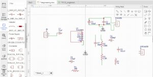
- new interface will be shown can be seen here
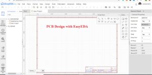
- Before making the project will have some understanding of the EasyEDA software tools and functions.
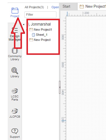
- First one is project option where you can see all details of projects that you have made in the software.
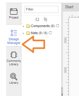
- Next is design manager where we can see details of all components used in our projects and wire used for making connections.
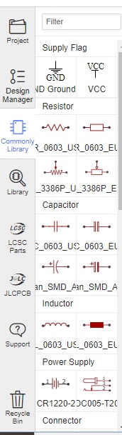
- Next component library where all components for the project can get to make a circuit diagram. Any project you can create from components get from this library
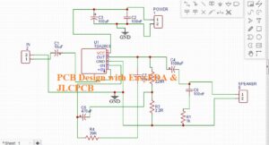
- After that know about the menus of software
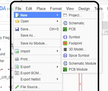
- First one is file tab from where you can create new or already made projects. With other features that are listed in the figure
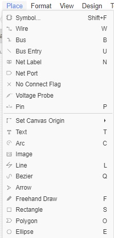
- Another one is the place tool that has wire, bus and different often used for projects.
- The design tool will use for the conversion of the schematic to PCB.

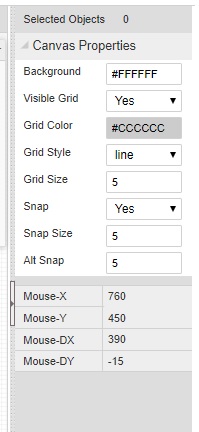
- In below figure the details of objects elected in the circuit can seen.
- Till now I hope you have get the detail overview of EasyEDA software that will help you to make the design. Now we will draw the circuit of our project that we are using for PCB design. The CIrcuit can be seen here
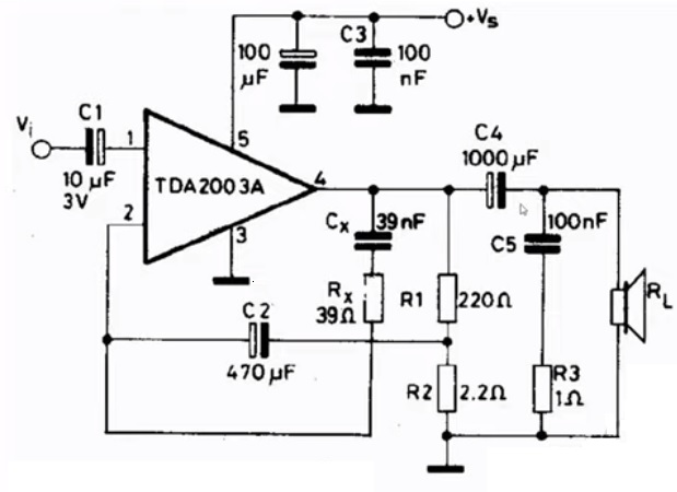
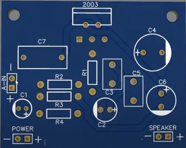
Project Components
- The component that we will use in the circuit are listed here
- capacitor 5 in number
- TDA2003A
- Resistances 4 in numbers
- Speaker as load
- All values of these components can be seen in the above figure
- Al these components of circuits are get from the component library can seen in the below figure.
- After that, all components connect according to the project’s circuit diagram and their respective value changes according to requirements.
- Now move to design tab and press on the convert schematic to PCB new interface will be displayed.
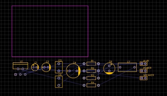
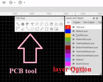
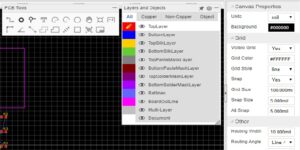
- In the below figure, you can see the PCB tools tab that will used to design the PCB. In the PCB layer window we can hide and unhide any layer also layer can be edited from here
- After that drag all components in the blue color rectangular box
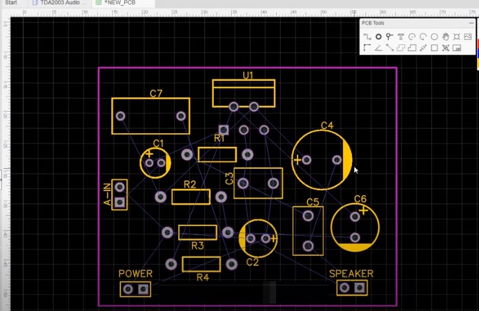
- Now use the autoroute option to get the resultant routing of circuit can seen here
- final look is like this
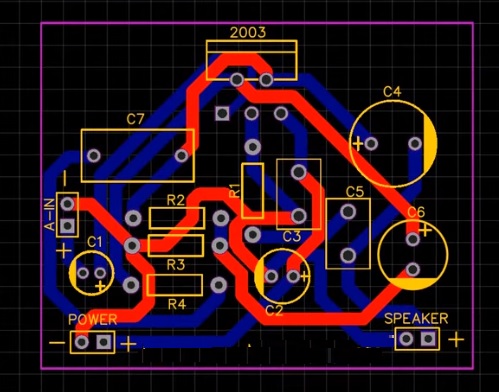
- Performing the all requirements final design of the circuit is this here
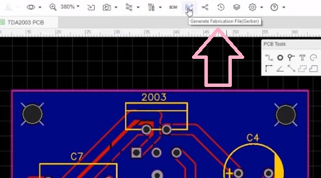
- Till now you have learned about the design of PCB and I have explained all the steps in detail. Now I will tell you how you can get the PCB from JLCPCB.
- For this purpose according to below figure press on the generate Gerber file option
- After that new box will open then you select the generate Gerber option
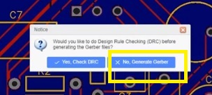
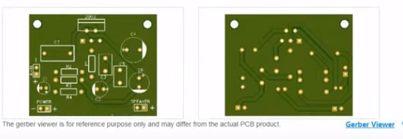
- When you press on the gerber file option then new window will open where you will come to your gerber file and the black rectangle box can use for further details.

- In the below figure you can see that there are two options first generate Gerber and the second one is order to JLCPCB. First one can use to download Gerber to save it for future use.
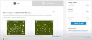
- A press on the order to JLCPCB directly your Gerber file will upload on the JLCPCB order form. can seen here
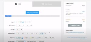
- Now upload the Gerber file to JLCPCB that can seen here and set the required parameters
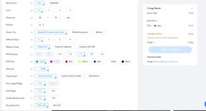
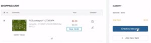
- When you adjust the all parameters to the board press on the add to cart button.
- On next page on the save to check out securely
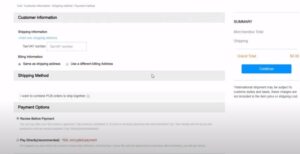
- On next page add your shipping address and shipping method
- So that is final over your final details for getting the PCB and designing PCB
- If you want to get details about how to get PCB from JLCPCB can visit this post detailed process has been explained.
HOW TO PLACE FIRST ORDER ON JLCPCB
- Your order of design has been sent to the JLCPCB based on projects requirements and time needed they will create you board and send to you
So, friends, I hope you have learned how to design a PCB board it is a very simple and basic process you must have basic knowledge of components and EasyEDA is the best free platform for students to design of PCB with great accuracy and fine result. After that the PCB consults the JLCPCB which is the best PCB supplier in the world and offers the best service regarding PCB. If you face any difficulty in designing PCB must visit the JLCPCB site. Further, if you have any queries ask in the comments. Thanks for reading have a good day


