
 Hello, readers welcome to the new post. Today we will discuss the Applications of Multilayer PCB. PCB board is a circuit board that is very commonly used in industries and different project creation. These boards are very commonly seen in electronic and electrical devices that have one or more copper layers. PCB board comes in different layers according to projects and design configurations such as a single layer, double layer, multiple layers, etc. The creation of a multilayer PCB design is a very important fact to getting the reliable operation and signal transmission through the proper operation. If the design is not accurate and the material for the substrate is not accurate then the required function can not be obtained which causes the noise in operation.
If the PCB board is designed accurately reduces electromagnetic emissions and crosstalk which enhances the operating quality. As the construction of multilayer PCB is high and not easy to find the faults existing in the board due to the multiple-layer complicated structure. But it provides good shielding and signal routing and offered numerous layout features for this board. In this post, we will cover the different parameters of Multilayer PCBs and learn about their practical applications. So let’s get started with Applications of Multilayer PCB
Introduction to Multilayer PCB
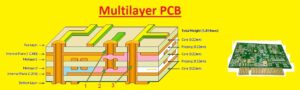
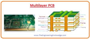
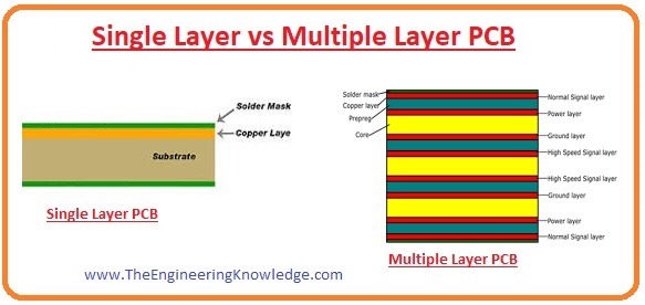
- Multilayer PCB is a type of PCB board that has more than two layers and a minimum of three conductive layers of conductive substance like copper material.
- When we analyze the structure of multilayer PCB then we will see that there is the same structure as the double-sided board but they have more layers about the core.
- The layer of these boards is connected through copper-plated holes and can be up to forty layers in multilayer boards.
- The component used for projects like a transistor, diodes, resistors, and other components are connected to upper and lower layers of board and other central layers are used for routing
- These boards have the ability to configure more components mostly used in different devices and projects normally up to 12 layers of boards are used.
- Different smart modules use 4 to 8 layers boards such as a mobile phone having 12 layers.
- The construction of a multilayer board has an even number of layers than the odds
- For 4 layer structure to enhance EMI operation signal layers must be positioned as close to plans and apply a larger core among the power and ground plane.
- The firm compiling among the signal trace and ground plane mostly decreases the place impedance that also decreases common mode radiation through a cable attached to PCBs. This close trace-to-plane coupling reduces crosstalk among the traces.
- For board having layers of about 12 needs a thin dielectric and that results in tight coupling among layers.
- These boards are used for the high-speed electronic operation to provide good EMI operation and signal quality.
- Tehre is no limit to the number of layers on board you can construct according to design and requirements.
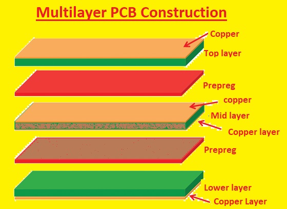
Multilayer PCB Construction
- To make the multilayer PCB there is first of all layout design created through the use of different design software like Eagle, Proteus Altium, etc.
- When the design is finished it is significant to make the internal layer core and laminate through require copper foil thickness, dry film, and ultraviolet light
- The next phase is internal layer creation, prepreg sheets, and copper foil sheet creation
- After that pressure is applied with heat and vacuum through a heated hydraulic press and it is significant to confirm that there is no air existing between layers. After that resins from prepregs connect sheets, core, and foil to make a multilayer board
- For multilayer PCB design designer is required to choose one layer for the ground plane and another for the power plane.
- In the case of digital PCBs, engineers can select the complete power layer and if there is an area on space at the upper and lower layer that can be employed for routing for extra power rail tracks
- Power layers exist in the central point of the board having ground close to the upper layer. When power is passes through internal layers remaining area is used for signal traces which have to rout
- There are two reference plans and signal via existing in these boards. Signal via permits electrical signals to pass through stacked plans used for routing
- The stitching via is attached to one plane next to the signal via and offered decrement in the area for signal flow
- In these boards, different types of vias are used to enhance the quality of routing like standard, blind, and buried vias
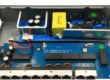
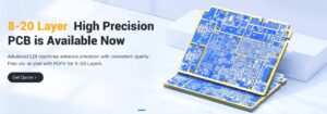
JLCPCB High-precision Multi-layer PCB
- JLCPCB is a high-level PCB-based service, provider. Founded in 2006, JLCPCB has been at the forefront of the PCB industry. With over 15-year continuous innovation and improvement based on customers’ needs, they have been growing fast and becoming a leading global PCB manufacturer, that provides the rapid production of high-reliability and cost-effective PCBs and creates the best customer experience in the industry.
- Whether you’re building your first printed circuit board or developing an electronic hardware product, they are here to help you build hardware easier and faster by providing a rapid PCB prototyping and PCB assembly service. They are constantly looking for new ways to improve and shorten the PCB prototyping process – from a pioneering online quote/order system, and automated manufacturing to fast delivery.
- JLCPCB currently provides a multilayer PCB service that has compatibility with twenty layers of the board. Multilayer boards are preferred for high-density board creation and in devices and projects that need accuracy and quality throughout the manufacturing process.
- So to fulfill all these features for your new project JLCPCB is the best option to get quality products at low prices.
JLCPCB Multi-layer PCB Advantages?
- The Multilayer PCBs of JLCPCB have many advantages.
- It is commonly used in complicated projects of electronic composite devices that have a high density of components and circuits.
- There is a need for more machines and details processes than other boards for the design and construction of multilayer PCBs. All these features enhance the chances to get high-quality boards. JLCPCB uses advanced solder mask LDI that provides reliable and stable solder mask bridges.
- There are no charges for “via-in-pad” with POFV for the 6, 8–20-layer circuit boards at JLCPCB. Free-of-cost POFV technique improves the efficiency of PCB design engineers. Since via has larger areas.
- As for these boards’ multilayer PCB stacks, layers exist on the upper side, so these boards can configure more components and circuits a small space than other boards which reduces the size and weight of these boards.
JLCPCB Multi-layer PCB Uses Advanced Solder Mask LDI
- JLCPCB as the best in all services so they make sure to use high-quality equipment for all high-layer count boards.
- JLCPCB is a famous manufacturer that uses LDI technology for multilayer PCB that is very less common to apply by other manufacturers.
- JLCPCB high-precision LDI features remove solder bridge problems. For a similar pad gap when the pad opening is one mil single die, the pad bridge can be 6.66 mils provided by the JLCPCB advanced LDI machine.
- So problems are solved through PCB design, in this way JLCPCB can deal with assembly irrespective of the density of the IC gap.
- Ulta high-precision alignment solder mask LDI is used for four to twenty-layer PCB orders, whether they are small batch or high orders, and either engineering charges are paid or not.
- Single and double-layer PCBs are monetarily created through CCD automatic alignment exposure instrument that does not compatible with these solder mask opening designs and has compatibility to multilayer designs four to twenty layers
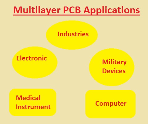
Multilayer PCB Applications
- The main applications of these boards are explained here
- These boards are used in mobile phones smart modules and some other electronic devices size they as the ability to handle more components on small structures.
- In a communication system, there are different conditions like high-temperature low-temperature pressure, and other factors to be faced by the component so these boards used in this industry
- This board provides durable operation and the ability to handle high pressure and temperature so used in industries and heavy machines
- Their robust and less weight functions help to use them in different medical devices and instruments like X-RAY machines etc
- These boards are used in military and defense instruments and machines used in the army.
- These boards are also used in the automotive and aviation industry.
Advantages of Multilayer PCB
- These are some advantages of multilayer PCB.
Small Size:
- The important feature of this PCB is that it is available in a smaller size.
- One of the most prominent and lauded benefits of using multilayer PCBs lies in their size.
- Due to their layer structure, multilayer circuit boards are characteristically lesser than other circuit boards with analogous functions.
- This features the most effective use of it for different engineering projects and electronic devices like phones, laptops, and computers.
Lightweight :
- Due to its smaller size, it also has fewer connections for large no of components which decreases its weight.
- Due to less weight, it’s the best option for current electronic devices.
High-Quality:
- The planning and designing used for the creation for this circuit board provide the best quality than the single and dual-sided printed circuit board.
Durability:
- The lifetime of this printed circuit board is longer than other PCBs. These boars do not twist its own until a certain external force is not applied.
- This board also can high temperatures and pressure.
Flexibility:
- Some multilayer printed circuit board has flexible behavior so it is known as flexible multilayer.
- It can be an extremely necessary feature for submissions where mild twisting and bending can exist on a semi-regular base.
More Powerful:
- This type of PCB is a tremendously higher-density structure, that has a large no of layers on a printed circuit board.
- These features make permit circuit boards to be further connective, and their inborn electrical belongings permit them to attain bigger capability and speed in spite of their lesser.
One connection point:
- The structure of this circuit board is like a single unit in spite of a large no of layers. So there is only one input connecting point and not for separately every layer.
- This feature is very helpful for usage in different projects that provide only a single point for input.
- This is also best for such devices that already have a smaller size.
- So it is most useful for the construction of mobile phones.
Multilayer PCB Disadvantages
- Now we describe some drawbacks of this PCB you must be aware of these disadvantages with the benefit of this board.
High Cost:
- The complicated design increases the price of this board more than the single-sided and double-sided boards.
- Its construction is a very difficult and time-consuming process, it also needs special techniques for construction and highly paid labor.
- It is one draws back that makes it costly that during its construction any mistake can lead to aging manufacturing of it and increases the price for labor and material.
- As this is a new invention for industries so some precautions are taken for its use in any project that makes it expensive.
- Due to all these causes, some other less costly option is also available.
Complex Production:
- Due to special manufacturing techniques, and special precautions its construction is more complicated than other PCBs.
- Due to that any minor fault on this board makes it wasteful.
Limited Availability:
- Its main drawback is that the machines required for its manufacturing are very expensive. Almost all PCB producers do not have the funds to buy these machines.
- Due to this, there are very less producers for this board production which make it expensive.
Skilled Designer Needed:
- As above we discuss that its design is very complicated so some highly skilled producers are required to construct this PCB board.
- If un-skilled men design-construct this board any smaller mistake in this board can cause serious problems in the complete structure.
Creation Time:
- As we discussed above its manufacturing is very complicated and needs special care so it takes a long time for its creation.
Benefits of Multilayer PCBs over Single Layer
- Now we discuss the comparison among the single-layer and multilayer printed circuit boards.
Higher Density:
- The density of a single-sided printed circuit board is less due to the lesser surface area, while the density of a multiple-layer PCB is higher due to a large no of layers.
- Due to this high density, this board provides a large circuit assembly, large capability, and high speed instead of a lesser size.
Small Size:
- Instead of large no layers, the size of the multiple-layer board is smaller which makes it effective for small-size electronics devices and due to the large size single-layer PCB is used for large-size devices.
Less Weight:
- Due to the absence of a soldering connection on multiple-layer printed circuit boards, its weight is less than the single-layer PCB.
How to Identify Different Layers in Multilayer PCB
- .To intensify layers of the multiple-layer board there are some points to be kept in mind.
- For instance, use a bright light to view copper planes that will guide you to view traces clearly and that make to find the internal layers.
- The internal layer can be seen easily when there are no lines or paths crossing the line of vision. For some boards number of layers is printed on the edges
Single-Layer vs Multi-layer PCBs
| Feature | Single-layer PCB | Multi-layer PCB |
|---|---|---|
| Number of layers | 1 | 2 or more |
| Cost | Low | High |
| Complexity | Simpl | complex |
| Design and production | Easy | difficult |
| Power | Low | High |
| Durability | Low | High |
| Applications | S calculators and toys | smartphones and laptop |
Why Multilayer PCB Mostly Used
- In different industries multilayer PCB is mostly used. Due to enhancement in the different options in the industry and the use of components I prefer this board.
- The single and double-layer board is limited in terms of board size and operation that has been covered by the multilayer boards.
- But with some advantages, there are some disadvantages use of multilayer boards over single and double layers such as expensive boards and design complications.
- But due to its good operation and working preferred instead of larger cost.
- With the use of new technology and machines, the creation cost of the board is also reduced with great benefits and advantages.
Related Posts
- Aluminum PCB (Printed Circuit Board)
- Multilayer PCB (Printed Circuit Board)
- Rigid PCB (Printed Circuit Board)
- Flex PCB (Printed Circuit Board)
- High Frequency PCB (Printed Circuit Board)
- Single Sided PCB (Printed Circuit Board)
- Rigid-Flex PCB (Printed Circuit Board)
- Double sided PCB (Printed Circuit Board)
Faqs
What is the basic knowledge of PCB?
- The PCB board comes with a rigid layout that has electrical circuits created with embedded metal surfaces known as traces and larger areas of metal known as planes. Components are soldered on board metallic pads that are connected with board circuits. That helps components to interconnected
What is the information about multilayer PCB?
Multilayer boards are electrical boards that come with two or more internal layers have a compact design, are used for multiple functions, are less weight, and are flexible and durable. It used in telecom, electronics, military applications
What is a multilayer PCB used for?
They are used for heart monitors, X-ray equipment, CAT scan equipment medical testing devices, etc
What are PCBs in engineering?
The PCB board’s electronic assembly uses copper conductors to make electrical connections between components. These boards offer support to the component connected in results devices mounted in the enclosure.
What type of engineer designs PCBs?
PCB designers are experts and professionals who have holistic responsibility for both electrical engineering and board design. They come in different operations such as schematic capture, embedded software development, routing layout, , component footprint creation, documentation, etc.
Do electrical engineers design PCBs?
Electrical engineers can make PCB designs but it is not the main part of their job description
How do I become a PCB design engineer?
- Learning basic electronics, knowledge of electronic components and their interfacing is the main skill to become a PCB designer some others are
- PCB knowledge
- PCB design software.
- PCB layer stack-up
- PCB design rules
- Mechanical design.
- Design review process
- Communication skills.
How long does it take to learn PCB design?
It depends on their abilities but normally 6 – 8 months to become a proficient PCB designer
That is all about the Applications of Multilayer PCB all details have been explained if you have any questions ask them here. Thanks for reading have a good day