 Hello, friends welcome to another technical post. I hope you all enjoying your life. In this post, we will have a detailed look at log and antilog amplifiers. These types of amplifiers are used in such applications where compression of analog input data occurs and in such applications were used for linearization of such transducer (it is a device that converts any type of signal into electric) which has exponential outputs, with that has analog multiplication and division.
These amplifiers also preferred for such communication systems where large value frequency is used like an optical fiber communication system which helps in the processing of various range signals. In this post, we will have a detailed look at their circuit working, operation, and some other parameters. So let’s get started with Log and Antilog Amplifiers.
What is Logarithm
- The logarithm of any number is the power that has such a number at the base that results in this number. The results generated by the logarithmic or log amplifier is directly proportional to the log taken of the input provided while the output pf the antilog amplifier is inverse of the input.
Logarithmic Amplifier
- The factor in a log amplifier is a component that shows logarithmic features which when exits in the feedback loop of the operational amplifier causes a logarithmic response.
- It indicates that the out signal is a function of the logarithm taken of the input signal and can be defined by this below-given equation.
Vout =-K ln(Vin)
- in this equation the K is constant and ln denotes the natural logarithm with base e. The natural logarithm is the power which has base that should raised in such a way that provides equal number.
- As we are using a natural log in the formulas every relation can be transformed in the log to the base 10 (log10) with the use of this relation
lnx =2.3log10x.
- The semiconductor PN junction in the shape of a diode or base-emitter junction of bipolar junction transistor offers logs characteristics.
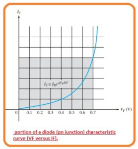
- As we know that diode show nonlinear behavior in forwarding a biased state up to the voltage range of 0.7 volts.
- In the below figure you can see the resultant curve in this curve VF is forward diode voltage and IF is forward diode current.

- You can observe that the diode cur is not linear in this graphical representation. The curve is not only non-linear it is logarithmic and certainly denoted by this given equation.
IF=IF IReqVF/kt
- The ln of multiple of 2 numbers equal the summation of ln of every number.
ln IF= ln IReqVF/kt
= ln IRq+VF/kT
ln IF – ln IR=qVF/kT
- The difference of these to numbers is equal to the ln of the quotient of terms.
ln(IF/IR)=qVF/KT
- By simplifying for VF we have
VF=(KT/q)ln(IF/IR)
Log Amplifier circuit having Diode
- If we connect a diode in the feedback circuity of the operational amplifier as you can see in the below figure.
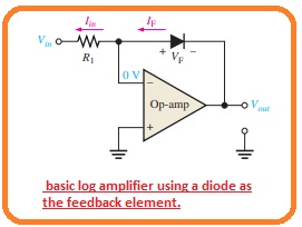
- Then we have a basic log amplifier configuration. As the inverting input is connected at the ground or zero volts the output is at -VF in case the input is positive.
- As the VF is logarithmic therefore is Vout. The output value is restricted to the extreme value since the diode logarithmic features are restricted to voltage value less than 0.7 volts.
- With that input should have a positive value in case od diode is linked according to the configuration shown above.
- For handling of the negative value of inputs, you should change the configuration od diode.
- The analysis of the circuitry is shown in the above figures is discussed as starting with the factor that Vout = -VF and IF=Iin there is no current exist at inverting input.
Vout = -VF
IF = Iin = Vin/R1
- Now we have
Vout =- (kT/q) ln(Vin/IRRI)
- The terminology kT/q is a constant value that is equal to the twenty-five milliVolts. So the value of output voltage will b.
Vout =-(0.025 V)ln(Vin/IRR1)
- By the above equation, you can observe that the output voltage is at the negative of logarithmic of the input single.
- The value of output is regulated through the value of the input signal and by varying the resistance.
- The value of IR non-varying for a resultant diode.
Log Amplifier connected with BJT
- The base-emitter junction configuration of BJT indicates a similar category of log feature as we discuss in the case of diode since it also has a PN junction configuration.
- The log amplifier having BJT has linked tot he common base configuration in the feedback loop as you can see in the below figure.
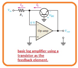
- You can see that the Vour according to ro the ground is equal to the -VBE.
- The analysis for this circuitry is like as for the diode log amplifier configuration except that VBE is replaced to the VF, IC is replaced with the IF, and IEBO is replaced to the IR.
- The relation between VBE and IC characteristic curve is given as.
IC= IEBOeqVF/kt
- In this equation, the IEBO is the emitter to base leakage current. The relation for the output is given as.
Vout=-(0.025 V)ln(Vin)/IEBOR1
Antilog Amplifier
- the antilog of any number is consequence taken when the base is raised to the power equivalent to the log of this number.
- To obtain the antilog you should take the exponential of the logarithm.
- The antilog amplifier is created by linking the transistor or diode at input according to the below-given configuration.
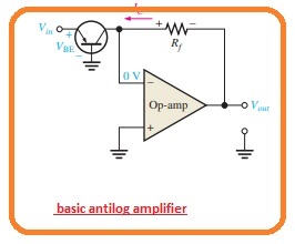
- The exponential formula is also applicable to the base-emitter pn junction.
- The output voltage is found through the current or feedback resistance.
Vout = -RfIC
- The features of this equation is given as.
IC=IEBOeqVBE/kt
- Now we have
Vout =IEBOeqVBE/kt
- We can onbserve in figure that Vin = VBE
Vout =IEBOeqVin/kt
- The exponential term can be defined as antilog as shown below.
Vout = -RfIEBOantiloga(Vinq/KT)
- As the kT/q is almost twenty-five mV.
Vout = -RfIEBOantiloga(Vinq/25mV)
How to compress Signal with Logarithmic Amplifiers
- In some special applications, the signal used can have a high amplitude and can not be applied to the application.
- the term dynamic range is mostly used for describing the voltage range comprises of the signal.
- In these conditions, the signal voltage can be reduced with the use of a procedure which is known as compression and it resultant is applicable to the system.
- If there is linear circuitry is used for reducing the amplitude the less voltage is compressed according to a similar percentage according to large value voltage.
- Linear signal compression mostly causes in the lessening the voltage disturbed with the noise and it is difficult to process to correctly decrease as shown in the below figure.
- To minimize this issue a signal having large-signal rance can be reduced with the use of logarithmic response as you can see in figure denoted as b.
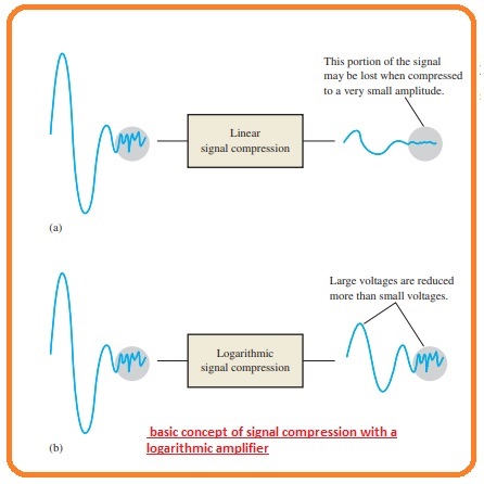
- In logarithmic signal compression, the larger voltage is decreased with a larger percentage than the less voltage and maintaining the lower voltage from lost in the noise.
Read also
- Difference Between An Operational Amplifier and Comparator
- What is LM709 Operational Amplifier?
- Difference Between Inverting and Non-Inverting Amplifier
- Introduction to MPSA06 NPN Amplifier Transistor
- Introduction to 2SC1345 NPN Amplifier Transistor
That is all about log and antilog amplifier if you have any query ask in the comments. Thanks for reading.