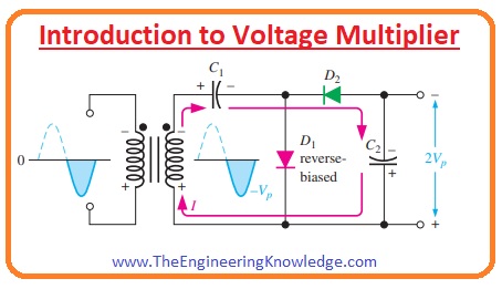
 Hello guys, I hope you are doing great. In today’s tutorial, we will have a look at Introduction to Voltage Multiplier. The voltage multiplier is also called AC to DC converter circuits and transformed less value of input signal into the high-value dc output. The main circuits elements of voltage multipliers are diodes and capacitors. These circuits are not new for electronic industries but have been used for numerous years. In 1932 first voltage multiplier was created by the Walton and Cockroft and had a rating of eight hundred kilovolts. With this invention, voltage multipliers have become very essential for such applications where high voltage and low-value current are needed. Application of these multipliers our circuits become simple as it reduces the use of a transformer.
As these circuits are constructed with the diode and capacitors and these components are connected in different arrangements. Due to these connection arrangement multipliers are categorized in different types such as doubler multiplier, tripler, and Voltage Quadrupler. In today’s post, we will have a detailed look at its working, circuitry and practical applications. So let’s get started with Introduction to Voltage Multiplier.
Introduction to Voltage Multiplier
- The voltage multiplier is rectifier circuitry that increases the amplitude of the input signal at output terminals than the input signal.
- With the use of amplifier circuits, we can generate less voltage to a high value of voltage for different instrument testing purposes.
Types of Voltage Multiplier
- There are 4 main types of voltage multiplier which are listed.
- Half-wave Voltage Doubler
- Full-wave Voltage Doubler
- Voltage Tripler
- Voltage Quadrupler
Let’s discuss them with the detailed.
Half-wave Voltage Doubler
- From the name of this multiplier, you can observe that the output of this circuitry will be two times the amplitude of input signal.
- This circuit consists of 2 diodes, 2 capacitors, and alternating current input supply.
- Let’s discuss this circuit for both halves of an input signal.
For Positive Half Cycle:
- The circuitry of half-wave voltage doubler is shown below. When a positive half of input signal is passing through the circuit diode D1 is in forward biasing condition and current flows through it.
- Due to this current of diode D1 capacitor C1 gets charged to a peak value of input signal that is Vm.
- While the diode D2 is in a reversed biasing condition so current will not pass through capacitor C2.
- So when the positive half comes to the circuitry only capacitor C1 gets charged while C2 remains uncharged.
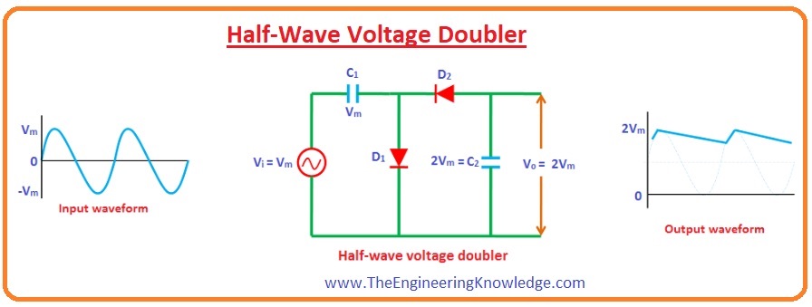
For Negative Half Cycle:
- When the negative half of input signal comes across circuitry then the diode D1 is in reverse biasing condition.
- Due to reverse biasing of diode D2 current will not flow through the capacitor C2 and it will not get charged.
- While the charge stored in a capacitor C1 during positive cycle will be released.
- But the diode D2 is in forward biasing condition for negative half cycle. Due to forward biasing condition of diode D2 current flows through it and capacitor C2 will get charged due to the current of Diode D2.
- The charge stored on the capacitor C2 will be equals to the 2Vm because charge across the diode C2 is the sum of the input supply voltage Vm and voltage due to capacitor C1.
- So during the negative half cycle voltage across the capacitor C2 is due to input source and capacitor C1 that is 2Vm.
- If we connect the load with the circuitry then the charged stored across the capacitor C2 will be used by the load and capacitor C2 will be discharged.
- When the next positive half-cycle comes across the circuitry diode D1 will again in forward biasing conditions current flows through it that will stored charge across the capacitor C1 and C2 will remain unchanged.
- But the charge stored (2Vm) in a capacitor during the first cycle was used across the output load.
- So we concluded that the voltage provided by the half-wave doubler is (2Vm) means two times the input voltage.
- So we can note that capacitor C1 and C2 are charging and discharging in half-wave doubler circuitry for alternating half-cycles.
Full-Wave Voltage Doubler
- The circuitry of full-wave doubler comprises an input ac supply, 2 diodes, and 2 capacitors.
- In the below figure circuitry of the full-wave doubler is shown.

For positive half-cycle:
- For a positive half cycle of an input signal, diode D1 is in forward biasing condition. Due forward biasing current will flow through the diode D1 and this current will charged the capacitor C1 to a peak value of input signal Vm.
- While the diode D2 is in reverse biasing condition for a positive half cycle of the signal.
- Due to reverse biasing current will not flow through the diode D2 and capacitor C2 will remain uncharged.
For Negative half-cycle:
- For the negative half cycle of input supply diode D2 is in forward biasing condition and current due to D2 charged the capacitor C2 to a peak value of input signal that is Vm.
- While D1 is in reverse biasing condition for the negative half cycle. No current will flows through this diode.
- So we concluded that both capacitor C1 and C2 will be charged alternatively for both half cycles.
- In the above circuit, you can see that the output of this circuitry is taken across the capacitors C1 and C2 that are connected in series.
- When there is no load is attached with the circuitry then the voltage across the circuit will be (C1 + C2 = Vm + Vm = 2Vm.)
- When there is load is attached to the circuit then the voltage at output terminals will be less than the 2Vm.
This circuitry is known as full-wave voltage doubler as one capacitor remains charged during every half cycle of input signal.
Voltage Tripler
- If we connect one more capacitor and diode in the circuit of half-wave doubler than we will have a voltage tripler circuitry.
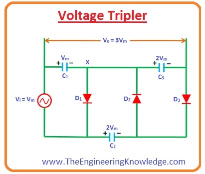
For first positive half-cycle:
- For ist positive half cycle of input alternating signal diode D1 is in forward biasing condition while other two diodes D2 and D3 are in reversed biasing condition.
- Due diode D1 current flows through the circuitry and it will charged the capacitor C1 to the value of Vm.
For Negative Half Cycle:
- For negative half cycle diode D2 is in forward biasing condition and diodes D1 and D3 are in reverse biasing condition.
- The current of D2 will be charged the capacitor C2 to a value of voltage double the input voltage (2Vm).
- While the charge stored in capacitor C1 is discharged. The voltage of capacitor C1 and input signal voltage Vm are shown across the capacitor C2.
CV1 + input voltage =(Vm + Vm = 2Vm)
For 2nd positive half-cycle:
- For 2nd positive half cycle of signal diode D3 is in forward biasing condition while other diode D1 and D2 are in reversed biasing condition.
- D1 is in reverse biasing condition as the voltage at point ‘X’ is negative due to voltage Vm across the capacitor C1 and D2 is in reverse biasing condition due to its direction arrangements.
- Due to this voltage (2Vm) about the capacitor C2 will releases. Due to the charge released by the C2 capacitor C3 will be charged have voltage value about the 2Vm.
- In the above figure, you can see that capacitor C1 and C3 are in series combination and output can get about these capacitors.
- The value of voltage about the capacitor C1 is Vm and voltage across C3 is (2Vm) so the total voltage at the output terminals will be equals to the sum of both capacitors voltages.
(C1 + C3 = Vm + 2Vm = 3Vm)
- From the above equation for can concluded that output voltage for this circuitry is equals to the 3Vm that is the three-time of an input signal.
Voltage Quadrupler
- If we include one pair of diode and capacitor in the tripler circuit than we get voltage quadrupler.
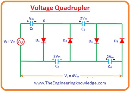
For Ist positive half-cycle:
- For Ist positive half cycle of input ac supply, diode D1 is in forward biasing condition while the other three diodes D2, D3 and D4 are in reverse biasing condition.
- So current will flow through the diode D1 and this current will charge the capacitor C1 to a peak value of input signal Vm.
For Ist negative half cycle:
- For the Ist negative half-cycle D2 is in reverse biasing condition and other diodes D1, D3, and D4 are in reverse biasing condition.
- The current will flows due to diode D2 and the capacitor will be charged due to this current.
- The value of voltage across the capacitor C2 will be double the input signal (2Vm).
- The voltage (2vm) across the C2 is due to discharging of capacitor C1 and input voltage Vm.
C1 voltage + input voltage = (Vm + Vm = 2Vm)
For 2nd positive half cycle:
- For 2nd positive half cycle of input signal diodes D1, D2 and D4 are in reverse biasing conditions. While diode D3 is in forward biasing condition.
- Due to the negative value of the voltage at point ‘X’ D1 is in reverse biasing condition but the D2 and D4 are in reverse biasing mode due to their connection arrangements.
- So capacitor C2 will release its charge that is 2Vm. This released charge stored at the plates of C3 and voltage across C3 will be 2Vm.
For 2nd negative half cycle:
- For the 2nd negative half cycle of input signal diodes, D2 and D4 are in forward biasing conditions while D1 and D3are in reverse biasing mode.
- Due to that C3 releases, its charge and this charge will store on the C4 voltage across C4 will be 2Vm.
- In circuit you can see C2 and C4 are in series combination and output also taken across these capacitors.
- As the voltage across capacitor C2 is (2Vm) and across C4 is also 2Vm So the net output will be equals to the sum of voltage across these two capacitors.
(C2 + C4 = 2Vm + 2Vm = 4Vm)
You can see the output of this circuitry is 4-times the input signal (4Vm).
So friends that is a detailed post about the voltage multiplier. I tried my level best to make easier for you if you have any further query about voltage multiplier ask in comments. Thanks for reading. Have a good day.