
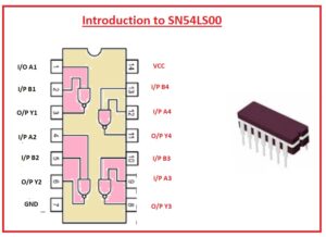
SN54LS00 Pinout
| Pin Number | Pin Name |
| 1,4,9,12 | NAND Gate Input pin (A) |
| 2,5,10,13 | NAND Gate Input pin (B) |
| 3,6,8,11 | NAND Gate Output pin (Y) |
| 7 | Ground |
| 14 | Vcc (Vdd) used to power IC about +5V |
SN54LS00 Features
- It has a dual input NAND gate and comes in quad packaging.
- It comes with a working voltage of five volts
- High-level output current is – 0.4 mA
- Low-Level Output Current value is about 4 mA
- Propagation Delay Time for this component is 15 ns
- Operating Temperature Range of this module is 55 C to + 125 C
- It comes in 14-pin PDIP, GDIP, PDSO packages
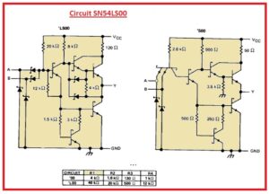
SN54LS00 circuit diagram
- It is 8 pin module and has 4 output NAND gates. This board is used for different electronic circuits. it is compatible to 2 and 4 inputs
- They can also used for logic inverter NAND gate configuration used to make not get combinations.
Circuit description
- In 2 input and 4 and gate structure comes with NMOS transistor with metallic oxide semiconductor field effect transistor at base pin and BJT at collector.
- The output of five volts is used for input TTL COMS.
- SN54LS00 also comes with an inner pulldown resistor that is used to set the Vcc value for controlling the output voltage.
- This board is also used for PWM controllers, PWM regulators, and feedback amplifier circuits.
- it has more features such as 3 state logic outputs and an inner pull-up resistor.
SN54LS00 NAND Gate Truth Table

Uses of SN54LS00 IC
SN54LS00 has 2 input 4 NAND gate IC and common part of different electronic circuits. It is used for NAND gate operation in different circuits. It is used for not gate combinations as well. It is used to make NOT gate combinations for different projects and is also part of high-speed NAND operations.
This chip comes with low transition times that are used for high-speed features and is also part for high-frequency systems.
Working of SN54LS00 IC
SN54LS00 comes with 12 input output inputs that are used for 4 NAND gates. For using this component provide power at Vcc and ground pinis.
The working voltage of the IC is about 5V and also has features to operate on 7V. The output voltage of the IC for pin Y is the same as the working voltage of the module.
According to the NAND gate truth table if both inputs of the gate are low output will be high and for other conditions is low.
Faqs
What is Quad 2 input NAND gate?
- 74LVC00A is a quad 2 input NAND gate that has input working from 3.3 V or 5 V. These features help to use as a transistor for conditions where 3.3 V and 5 V are used. Schmitt-trigger process at inputs that make slower input rise and fall times.
What is the IC number of 4-input NAND gate?
- 74HC20 is 14 pin Quad 4-Input NAND Gate integrated ciorucit. This component comes with 4 independent gates each used for different logic NAND function.
What is the Quad 2 input OR gate IC number
- 74LS32 (or 7432) IC-OR Gate-Quad-2 Input
Is a quad two-input OR gate IC 7432?
- 7432 is a 14-pin Quad 2 input OR Gate IC. The 7432 offers 4 independent 2 input OR gates having standard push-pull outputs. it is designed to work for a power supply range of 2.0V to 6.0V.
What is the difference between 74 and 54 series in IC?
- 74 in name if IC number like 74LS04 denoted commercial temperature range. The 54 is used to show the military temperature range.
How many 2 input NAND gates are there?
- The number of 2 input NAND gates needed to use 2 input XOR gates is four. Like the number of 2-input NOR gate needed to use a 2-input XNOR gate is 4.
How many transistors in a 4 input NAND gate?
- The NAND gate is one transistor for input. THe NOR gate has one transistor per input, AND the gate is a NAND gate and note gate so it get one transistor more than the NAND gate. Some are OR vs NOR.
What is the IC number of Quad 2 input or gate?
- 74LS32 is a dual input OR gate that comes with quad packaging. it has 4 gates and that performed logic OR operation. every gate comes with two inputs so it is called Quad 2-Input OR Gate.
How many pins does SN74LS00 have?
- 14 pinouts
What is the difference between 74HC00 and 74LS00?
- The basic difference between HC and LS of chip type is that 74HC00 is compatible to 2V to 6V and 74LS00 can work for five volts. After connection, we can use any 4 NAND gates inside.
Read also


