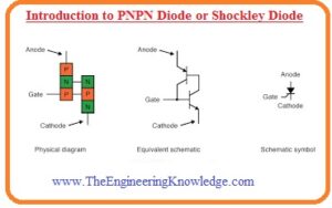
 Hello, friends welcome to new post. In this post, we will have a detailed look at Introduction to PNPN Diode or Shockley Diode. The PNPN diode is also called Schockley diode due to its creator scientist William Shockley. It comprises of 4 layers of semiconductors. The p and N layers are assembled in alternative manners. With disconnected gate configuration, it is like to the thyristor. This diode offers negative resistance characteristics.
The first time in 1950 it was created in Schockley semiconductor laboratory. In this post, we will discuss its working, structure, and related factors. So let’s get started with Introduction to PNPN Diode or Shockley Diode,
Introduction to PNPN Diode or Shockley Diode
- The semiconductor created through the 4 layers is generally called thyristor. The member of this group is known as PNPN or trigger diode.
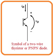
- The symbolic representation of the PNPN diode can see here.
- The PNPN diode is a rectifier configuration having offered the voltage-current characteristic in forwarding biased region.
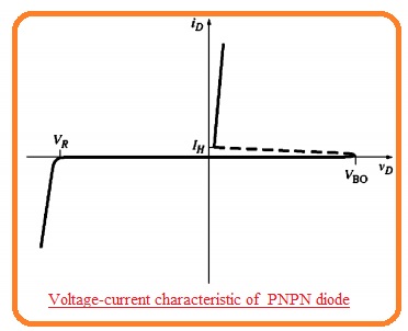
- The voltage characteristic of the PNPN diode can seen here.
- There are 3 parts of this characteristic region
- Reverse-blocking region
- Forward-blocking region
- conducting region
- In the reverse blocking region PNPN diode operates like the normal diode and stops the reverse voltage.
- In the case of conducting region, the PNPN diode also operates like a normal diode permitting a high value of current at less voltage loss.
- The main difference between normal diode and PNPn diode is the forward blocking diode.
- In the forward biased state, there is no movement of current till the forward-biased voltage loss are larger than the specific value called breakover voltage VBO.
- In case when the forward voltage about PNPN larger than VBO the PNPn diode gets on and stays in this state till the current passing in it less than the specific value.
- If the current is less to this certain value that called holding current IH the PNPn diode becomes off and will not operates till the forward voltage loss larger than VBO,
- The PNPN diode gets on when the voltage provided VD is larger than VBO.
- It gets off when the current ID is less than IH.
- it stops all current passing in the reverse direction till the extreme reverse voltage is high.
PNPN Diode Working
- Contrary to normal diode there is more than one PN junction Schocllley diode. The structure of this diode comprises 4 parts of semiconductor linked in alternative fashion among anode and cathode terminals of PNPN.
- As there are more than one junctions in this diode but due to 2 terminals, it called a 2 terminal device.
- The Shockley diode retains in off condition having a high value of resistance till voltage of larger value than the trigger voltage is given at its terminals.
- In the case of voltage larger than trigger value the resistance losses to very less value and it gets on.
- There are constituent transistors is used in the on and off condition. As there is a resemblance to pairs of connected bipolar transistors first is PNP and the second is NPn no transistors get on till the second is on due to the absence of current passing through the base-emitter junction.
- A certain value of voltage is given and out of 2 one transistor get breaks down. It starts operating and permits the base current to move to the second transistor in results the saturation of both transistors retaining both transistors in one condition.
- At decreasing the voltage to a certain low level the current passing changes to very less value to retain the transistor bias.
- Due to the very less value of the current one transistor will move to cut off state causing the base current disturbance at the second transistor in results both transistors become off condition.
PNPN Diode Electrical Parameters
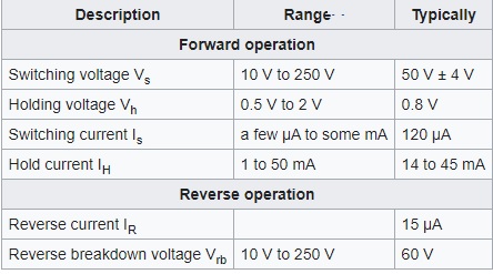
- The PNPN diode parameters are mentioned here.
FAQS
What is a Shockley diode also known as?
- It is also called a PNPN diode or 4-layer diode that works like a normal diode without triggering inputs. In reverse-biased conditions, no current flows in it, and in forward-biased conditions, current flows in it if the voltage about it is higher as compared to the breakover voltage.
What is the difference between P and N junction diodes?
- The PN junction diode is the basic type of semiconductor diode. It is made with the connection of two types of semiconductor materials, P type and N type, to make a junction. The P materials have high holes that are positively charged, and the N-type materials have electrons that are negatively charged.
Are Schottky diodes and Shockley diodes the same?
- The Shockley diode is an SCR with a gate not configured. In Schottky diode semiconductors and metals like molybdenum, they are configured differently than PN junctions for making a forward voltage of 150 to 450 mV.
What is the difference between SCR and Shockley?
- The silicon-controlled rectifier is a Shockley diode with an extra pin configured. That extra pin is called a gate and is used for triggering the device in conduction through the use of a small voltage.
What are the characteristics of a PNPN diode?
- It comes with 4 4-layer diodes and works like a normal diode without trigger inputs in reverse biased conditions. No current passes through it, and in forward biased current flow, it has a high value that breaks over voltage.
That is a detailed post about PNPN diode if you have any further query ask in the comments. Thanks for reading. have a nice day


