
 Hi, reader welcome to the new post. In today’s post, we will have a detailed look at Introduction to PIC12F675. It is a type of microcontroller which is eight-bit PIC MCU created by the MIcrochip. There is flash memory is assembled on this board. This type of PIC MCU comprises of eight pinouts that is less than other PIC controllers that have twenty and in some cases forty pinouts.
In today’s post, we will discuss the features, pinouts, working, and some other related factors. So let’s get started with Introduction to PIC12F675.
Introduction to PIC12F675
- The PIC12F675 is eight-bit MCU that is manufactured by the Microchip technique and created at the RISC (Reduced-instruction-set Computing) structure.
- Due to less expensive and small dimensions, it is most preferred by the engineers for project construction.
- Like other microcontrollers, this controller does not use SPI and I2C protocol for communications.
- This module has a program memory of having a space of 1.7-kilo byte with that has random access memory of sixty-four bit and EEPROM of one twenty bytes of.
- At this module, 2 timers of eight and sixteen bits are designed on this board.
- For comparison of two signals, there is single comparator is used at the board.
- The voltage over which it operates is between two to 5.5 volts.
Features of PIC12F675
- These are some important features of PIC12F675.
- There is analog to digital converter having four channel with the eight-bit resolution is exist on this board.
- There are 2 timers of eight-bit and sixteen-bit is used at this board.
- Random-access memory of sixteen bytes is used at this board.
- The voltage over which this board operates is 2 to 5,5 volts.
- It does not use pulse width modulation.
- It uses a single comparator.
- It also has an exterior oscillator of having a frequency of twenty megahertz.
- There is an inner oscillator of four megahertz is exists on this board.
- This module comprises of the eight-bit central processing unit.
- There is eight pinouts of this board.
- There is six pinouts out of eight which can be a program easily.
- Instead of SPI and I2C, this module uses the ICSP protocol for communication.
- There is a flash memory of two-kilo byte is assembled on this board.
- The value of extreme in current is twenty-five milliamperes and out current is twenty-five milliamperes.
- The temperature over which it operates is minus forty to plus one twenty-five centigrade.
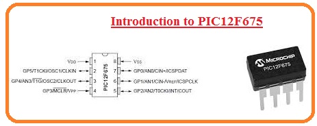
Pinout of PIC12F675
- The main pinout of this board is described here.
VDD
- At this pinout positive supply is provided.
GP2/AN2 /T0CKI/INT/COUT
- It is general-purpose pinout two, analog input two, a timer clock input, exterior interrupt, and for comparator output.
GP1/AN1/CIN-/VREF/ICSPCLK
- It is general-purpose first pinout, used for analog input one, comparator input.
GP0/AN0/CIN+/ICSPDAT
- This general-purpose pinout used as a comparator input.
GP5/T1CKI/OSC1/CLKIN
- These five general-purpose pinouts which used as oscillators, timer clock, and exterior clock source input.
GP4/ AN3/ T1G/OSC2/CLKOUT
- The GP4 is four general-purpose input and output pinouts. AN3 are analog input three pinouts and OSC2 are oscillator pinout.
GP3/MCLR/VPP
- it is general-purpose input and output pinout three used for master clear input or Reset pinout and to program voltage.
VSS
- This used as ground pinout.
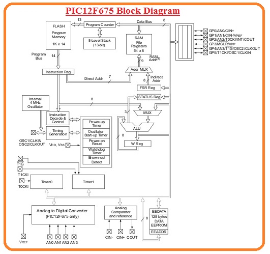
PIC12F675 Block Diagram
- In the below figure you can see the block diagram of PIC12F675.
Applications of PIC12F675
- These are some applications of this module.
- It used in different types of displays like scrolling display, temperature monitors,
- It used in an embedded system.
- Different types of security system use this board
- In medical devices, this module is used.
that is a detailed post about PIC12F675 if you have any further query ask in comments, Thanks for reading. Have a good day.