 Hello friends, I hope you all are doing great. In today’s tutorial, we will have a look at Introduction to Phototransistor. The phototransistor is such electronic deceive that used to operate on light for switching and amplification process. It consists of three layers of semiconductor material and its base is a light-sensitive region. Its base part absorbs light and transforms into the current that moves from collector to emitter.
The physical structure of phototransistor is like the normal transistor but it does not have a base like another transistor. In place of base current, it uses light as an input. In today’s post, we will have a detailed look at its working, construction, applications and some related parameters. So let us get started with Introduction to Phototransistor.
Introduction to Phototransistor
- The phototransistor is like the bipolar junction transistor with the difference is that in phototransistor base current is generated and regulated through the light in place of a voltage source.
- The main function of phototransistor is that it transforms light into electrical energy.
- Base current of phototransistor is generated when light strikes on the light detecting part of base.
- In the structure of the phototransistor lens incident, the light on the collector-base Pn junction.
- When no light falls on the transistor there is only a small amount of thermally produced collector to emitter leakage current ICEO usually this current in the range of neno amperes.
- When light falls on the collector base pn junction as the base current is generated that denoted Iλ and directly proportional to the intensity of light.
- Due to that collector current is increased with the Iλ.
- Phototransistor operates like the normal bipolar junction transistor with a difference of base current generation process. In numerous cases, there is no electrical linking to the base.
- The light which produces base current and collector current is related through the given below equation.
IC= βDCIλ
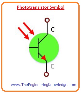
- The symbol and some normal phototransistors are shown in the below diagram.
- In this transistor generation of base current through light occurs in the collector-base junction region if this area increases the generation of base current will also increase.
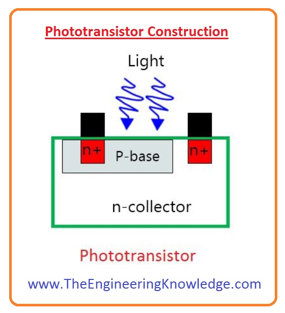
- Therefore, a distinctive phototransistor is created to provides a large area for the incident of light. The below figure also shows the structure of the photoresistor.
- This electronic component has usually two or three terminals.
- In three terminals arrangement base terminals is used to operate photoresistor as normal BJT.
- In 2 terminals arrangements, the base is not present so it used only on the light as input.
- Most of the application uses 2 lead configurations of a phototransistor.
Phototransistor Symbol
- The symbolic representation of phototransistor is like the normal transistor.
- The difference is that it has two arrows that indicate the incidence of light.
Phototransistor Working
- This transistor is created with the semiconductor substance. When light falls on the semicondutor material due to that holes and electrons pair created and base current flows.
- The main function of the base is to biased the transistor.
- When light falls on the base pairs of electrons and holes created. This paring of holes and elections occur during reverse biasing conditions.
- the flow of electrons due to exterior voltage source generates the base current.
- This base current moves to the emitter of the transistor.
- The main disadvantage of this transistor is that it has less frequency response.
Phototransistor Construction
- The construction of a phototransistor is similar to the not transistor. At earlier days silicon and germanium were used for the construction of photransistor.
- A small size hole is created on the collector-base junction to place lens.
- This lens is used to focus the light on the surface.
- Currently, a transistor is created with the gallium and arsenide which are highly effective.
- The emitter-base junction of a diode is in forward biased and collector-base junction is in reverse biased condition.
Phototransistor Characteristics
- These are some characteristics of a phototransistor.
- Its price is less and used for infrared photodetector.
- It exits with the gain of a hundred to above fifteen hundred.
- Its response is high.
- It offers different packaging such as epoxy coated, transfers molded and SMT.
Difference between Photodiode and Phototransistor
- These are some differences between phototransistors and photodiodes.
Photodiode:
- Photodiode is a type of diode that generates current when light falls on it.
- It generates a current.
- Its output response is high.
- It is a less sensitive device.
- It can be biased both forward and reverse.
- It used in solar panels.
Phototransistor
- It is a transistor that transforms light into electrical power.
- It produces both current and voltage.
- Its output response is less speed.
- It is a highly sensitive device.
- It used in a smoke detector, compact disc, laser.
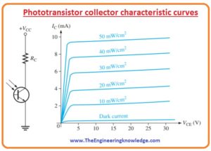
Phototransistor Collector Characteristic Curves
- In the below figure you can see the biasing circuit and collector characteristic curves.
- You can see that every curve on the graph is dependent on the light intensity and collector current increases with the intensity of light.
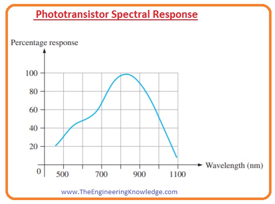
- This transistor does not conduct for all types of a wavelength of light but for a certain range.
- It mostly operated for red and infrared light.
Phototransistor Applications
- These are some important applications of a phototransistor.
Relay circuits Driven by Phototransistor
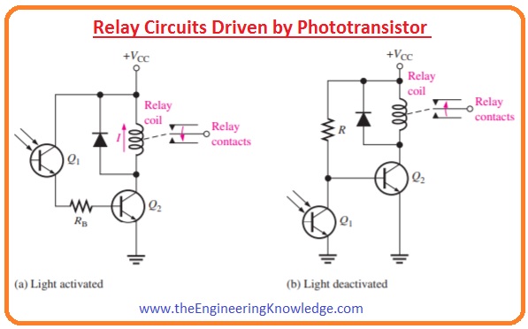
- In the below figure circuit denoted as (a) shows the light operated relay circuit.
- In this circuit, phototransistor denoted Q1 runs the bipolar junction transistor Q2.
- When a certain amount of light falls on the photrantsistor Q1 BJT Q2 goes into the saturation and collector current operates the relay.
- The diode around the relay coil stops, by its limiting process, a huge voltage transient from occurring at the collector of Q2 when it turns off.
- In figure circuit denoted as (b) shows the deactivation of the relay through the incidence of light.
- When the incident light is not enough Q2 is in biased on the state, keep the relay energize.
- When the light is sufficient Q1 is in on state that make the base of transistor Q2 low due to that Q2 turns off and relay get de-energize.
Optocouplers
- In the packaging of the optocoupler LED is optically linked with the photodiode or phototransistor.
- In the below figure 2 simple types of optocoupler shown first have led to the photodiode and second has led to phototransistor packaging.
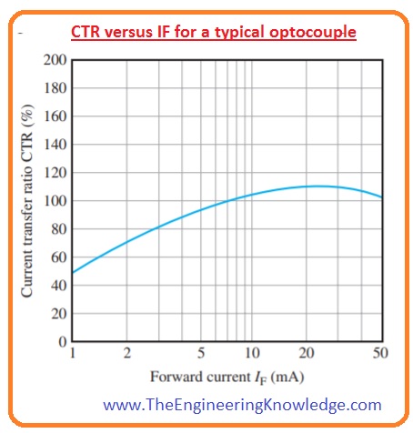
- The main factor in optocoupler is CTR or current transfer ratio. It is the parameter that defines how effectively a signal is linked from input to output.
- It is the ratio between the variation in the led current to the resultant change in photodiode or phototransistor current. It is typically stated as a percentage.
Phototransistor Advantages
- These are some advantages of a phototransistor.
- It generates a large amount of current than the photodiode.
- Its price is less, small size and easily assembled in the IC of a computer chip.
- It is a high-speed operation device and gives almost instantaneous results.
- It generates voltage while phototransistor can not do so.
Photoransistor Disadvantage
- These are some disadvantages of a phototransistor.
- The transistor created with the silicon is not able to handle voltage larger than the thousand volts.
- This device also not good for surges of the electrical signals.
- The current does not flow freely through this module.
Read also
- Transistor Symbols | Definition, Terminals & Operating Condition
- Siren Circuit using 2N2907 Transistor
- Introduction to BC108 NPN Transistor
- 2N3702 Transistor Working & Application
- Introduction to BC817 Transistor
- Introduction to BC847 Transistor
- Introduction to S9013 transistor
So, friends, it is a detailed post about phototransistor if you have any further queries about this module ask in comments. thanks for reading.
