 Hello, readers welcome to new post. Here we will give a detailed overview of the Introduction to PCB Reverse Engineering. The process through which design and fabrication is done through the use of existing boards by changing the functionality is called reverse engineering. Data obtained through this process is helpful to re-manufacturing, redesigning troubleshooting, and testing of modules used in strict conditions
There are numerous PCB manufacturing that offer PCB services with different features PCBWAY is one of the best that also helps its users with PCB reverse engineering and other PCB-based projects. To resolve all complications existing in reverse engineering you must need of any extra help. Either you have to update your older PCB design and make the new one then you must visit PCBWAY.
PCBWAY offers the high-quality boards than others. They provide all types of boards that you needed also offer the PCB prototyping services. Prototyping boars created by these PCB suppliers are mostly used in different projects. They are well-equipped and professional in all services.

Introduction to PCB Reverse Engineering
- PCB reverse engineering is a multilayer technique comprised of specific PCB research analysis and design of board re-creation.
- This technique is helpful to get the designing configuration of modules with its functional behaviors and features of the structure.
- This information helps any manufacturer to make new products that have the same features and structures but have some dissimilarities.
- The main objective of this technique is to get the details of design and different paramerts of any products. Such products that are designed can not be easily made effective through this process.
- A commonly used technique for reverse engineering is to disable the products and get the details of the structure.
- After that documents about the analysis is get and discussed with other engineers to make that product.
- By using this information manufacturers made the new products with good quality and features that older one have.
- Reverse engineering enhances the functions and quality of boards created by the manufacturers.

Advantages of PCB Reverse Engineering
- Numerous benefits can be obtained from this technique and different manufacturers create products that have great features. Some advantages are discussed here

The Durability of Important PCBs
- This process helps to maintain the outdated boards since if boards are damaged and not work for a long time and have to change. If you do not have a budget and techniques for a new board then reverse engineering will help you to maintain that significant board to work for long time intervals.
Get Data from Board Structure
- Most boards have details on the documents for processing but some boards do not have these documents so for this purpose structure of the board is used to get the details about the board and the creation of the new board.
Experts Dependency decreases
- Sometimes any faculty comes in the board and you need an expert engineer to solve it and may you not have access to them. In result, you need a reverse engineering technique to solve this issue and resolve the faults of the board
Finds Defaults in Other Manufacturers
- Any manufacturer of PCB always wants to make the best board than other manufacturers so reverse engineering helps you to make an effective and good quality board than other producers.
Make Less Expensive Boards
- Reverse engineering helps manufacturers know about the prices of other boards and through this process, you can make less expensive boards have the same quality since some companies charge higher prices due to less competitors
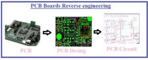
PCB Boards Reverse engineering
- There are some steps to follow for reverse engineering of PCB boards

Make Picture of PCB
- First of all make a picture of PCB board. this picture must be from both sides of the board and also from a dark background.
- From the holes on the board, nothing can be visible behind the holes and a clear picture gives great results
- Make sure to use of a high-quality camera to get a clear image. PCB must be well-lit
Image upload in Software
- After making the pictures uploaded in the software used for reverse engineering. Before uploading the image make it clear and crop to remove unnecessary details.
- There are different software existing that will help you make clear and edit your image.
Layout Creation
- The image was created then uploaded in the reverse engineering software and the three-dimensional schematic of the board.
- This structure of the board tells about the circuits working and electromagnetic field distribution. This schematic also helps to view the details of the component attached conductive components and the configuration of the trace
Make PCB Schematic
- Now construct the PCB schematic it will help us to view all the details of the components connected and the circuit design.
- The layout then takes the assembly of 2 dimensional CAD assembly structure. These 2D structures give details about the component’s connections and their operations. Getting hit layout details overview of PCB boards is obtained to make new ones with great quality and less expensive.
- You can also visit PCBWAY to high-quality boards with reasonable prices since they are equipped with professional engineers and tools that are commonly used.
Read also:
- PCB Plating Techniques: A Complete Guide for Quality and Efficiency
- Comprehensive Guide to PCB Voltage Regulators: Types and Applications
- PWB vs PCB: Differences and Similarities
- Matte vs Glossy in PCBs
That is all about PCB Reverse Engineering all details have been explained if you want to get further information and facing difficult let me know in the comments box we will help you to resolve your problems, Thanks for reading


