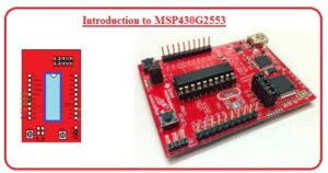
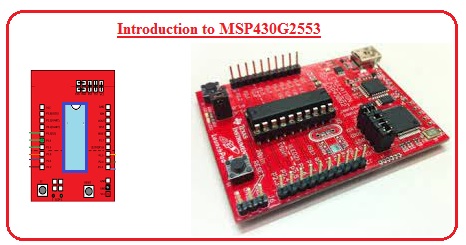
 Hi, students welcome to another interesting post. In today’s post, we will have a detailed look at Introduction to MSP430G2553. This controller belongs to the group of controllers that is MSP430. It uses less power and comprises of different types of features and components. The structure of this board comprises of 5 less power-consuming modes that help to increase the operating life of the battery.
This controller has a sixteen-bit central processing unit, registers and for extreme coding efficiency, there is a constant generator that exists on this board. In today’s post, we will discuss its working, application, pinouts, and some other related features. so let’s get started with Introduction to MSP430G2553.
Introduction to MSP430G2553
- The MSP430G2553 belongs to the microcontrollers which operate on sixteen bits and comprise of flash memory for storage of data.
- With the flash memory, there is random access memory is exists on this board, and the central processing unit of sixteen megahertz frequency is also created at this board.
- There is a ten-bit analog-to-digital converter of ten channels that comes on this board, and it also has capacitive touch-enabled input and output that exist on boards.
- For communication with other types of controllers and some exterior devices, it uses universal serial communication interfacing.
- There is a Launchpad kit supported with dual inline packaging that exists at this board which comprises almost twenty pinouts that help to interface different types of devices.
- It provides to linking the entry-level components with the board.
Features of MSP430G2553
- These are some important features of this board that is described here in detail.
- The range of voltage over which it operates is 1.8 volts to 3.6 volts.
- the communication protocol that it uses is USCI or universal serial communication interfacing.
- it has an active mode of two-thirty microampere at one megahertz frequency.
- Its standby mode current is 0.5 microampere.
- It off mode occurs at the current value of 0.1 microamperes.
- 5 power-saving modes exist on this board.
- It takes almost 0.1 microseconds to come to wake mode from standby mode.
- There are 2 timers of sixteen-bit with 3 registers are exist on this board.
- Twenty-four pinouts are operating as inputs and outputs exist on this board.
Pinouts of MSP430G2553
- The main pinouts of this board are described here with detail,
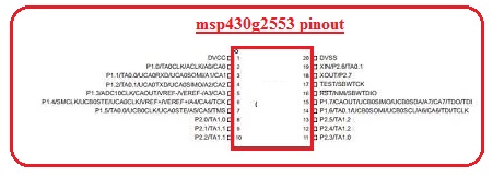
P1.0
- This pinout is operated as a digital input and output pinout.
TA0CLK
- At this pinout clock signal as input is provided.
ACLK
- Though this pinout A-clock signal is taken out as output.
A0
- This pinout is used as an analog-to-digital converter analog input.
CA0
- This pinout is linked with the comparator.
P1.1
- This pinout is operated as general-purpose input and output.
TA0.0
- The timer is connected to the pinout.
UCA0RXD
- At this pinout UART mode of communication is linked.
UCA0SOMI
- At this pinout, the SPI protocol of communication is used.
A1
- This pinout is operated as an analog to a digital converter input pin.
CA1
- This pinout is operate as comprator.
P1.2
- This pinout is operated as a general-purpose input and output pinout.
TA0.1
- At this pinout, the timer is linked with the board.
UCA0TXD
- This pinout is used as a UART protocol of communication.
UCA0SIMO
- Through this pinout, SPI protocol of communication is attached.
A2
- This is analog to digital converter pinout.
CA2
- This pinout is used as a comparator.
P1.3
- This digital input and output pinout is digital.
ADC10CLK
- This is analog to digital converter pinout.
A3
- this is analog to digital converter pinout.
VREF
- This reference pinout here reference voltage with negative polarity is provided.
CA3
- This pinout is used as a comparator.
CAOUT
- This pinout is used as comparator.

Faqs
What is MSP430G2553?
- MSP430G2553 is an ultra-low power mixed signal controller that has a 16-bit timer, 24 I/O capacitive touch-enabled pins, an analog comparator, and built-in communication features through the use of universal serial communication interfacing.
What is MSP430’s application?
- It is mostly used for energy meters, medical devices, and sensors operating without wires.
What is the current consumption of MSP430G2553?
- The power consumption feature of this module is 380 uA at 1 MHz at 3 volts.
What language is MSP430?
- It is configured with assembly language certain syntax based on assembler. The program is converted in assembly language into machine code.
What are the security features of MSP430?
- MSP430 comes with RTC-C modules and some security features for detection and recording tampers in the MCU. These pins are connected with an external mechanical switch for detection of when the enclosure is opened.
What are the operating modes of MSP430?
- LPM0: CPU is disabled.
- LPM1: loop control for the fast clock (MCLK) disabled.
- LPM2—fast clock (MCLK) is disabled.
- LPM3—the DCO oscillator and its DC generator are also disabled.
- LPM4-CC oscillator is disabled.
What processor does MSP430 use?
- MSP430 is a 16-bit processor with a non-Neumann architecture made for low power requirements. The CPU is defined as a reduced instruction set computer. address and data buses are 16 bits wide.
What is the architecture of MSP430?
- MSP430 comes with 7 features for address operands. 4 are applied in the CPU, 2 are due to the use of a program counter for registers, and one is indexing a register that has zero (status register).
What is the memory structure of MSP430?
- MSP430 memory is divided into 512-byte flash components. Based on type, the MSP430 comes with two components having 128 bytes or four components having 64 bytes. These components are called information memory.
What is the spec of MSP430G2553?
- Supply Voltage Range: 1.8V to 3.6V
- Ultra-low power consumption
- 5 energy-saving modes
- Ultra-fast wake-up from standby mode in less than 1μs
- 16-bit Reduced Instruction Set (RISC) Architecture, 62.5ns Instruction Cycle Time
- Basic clock module configuration
- Internal frequency up to 16 MHz with four calibration frequencies
- Run Mode: 230µA at 1MHz and 2.2V
- Standby mode: 0.5μA
- Off Mode: 0.1μ
- Internal ultra-low power low frequency (LF) oscillator
- 32 kHz crystal oscillator
What is the input voltage of MSP430G2553?
- 1.8 to 3.6 V
What are the characteristics of MSP430?
- Low power consumption:
- 0.1 μA for RAM data retention;
- 0.8 μA for real-time clock mode operation
- Low operation voltage (from 1.8 V to 3.6 V).
- < 1 μs clock start-up
- < 50 nA port leakage.
- 250 μA/MIPS at active operation.
What are the different types of timers in MSP430?
- MSP430 series chips come with 2 types of timers called Timer_A and Timer_B. They are 16-bit timers that have many captures that compare channels and selectable clocks.
- Timer B is complicated as compared to timer A and provides good interrupt features and has features to capture larger channels.
What is the arithmetic logic unit of MSP430?
- The MSP30 CPU comes with an ALU that performs addition, subtraction, comparison, and logic functions such as AND, OR, and XOR operations.
- ALU operation has affect on overflow, zero negative, and carry flags of register.
So friends that is a detailed post about MSP430G2553 if you have any further query ask in comments, thanks for reading. Have a good day.