 Hi students I hope you all are doing great. In today’s post, we will have a detailed look at Introduction to ATmega8. This type of microcontroller was the first time created in 1996 and eight-bit controller based on the CMOST technique and member of AVR (Advanced Virtual RISC) group of controllers. Its structural arrangement based on the RISC or reduced instruction set computer architecture.
in small-size assembly, it performs numerous functions by providing us from a spending amount to buy exterior components that are already assembled on it. In today’s post, we will have a detailed look at its working, features, applications, and some other related parameters. So let’s get started with Introduction to ATmega8.
Introduction to ATmega8
- The ATmega8 is created through the Atmel. It comprises of Harvard structure which functions with the RISC.
- The packaging in which it exits is three in number and is PDIP, MLF, and TQFP. There are twenty-eight pinouts of PDIP configuration and MLF and TQFP have thirty-two pinout configurations.
- It uses flash memory of eight Kilobytes for storage with comprises of one kilo RAM and five twelve bytes EEPROM.
- Some other factors this module has are a watchdog timer, brown out sensing, and 5 sleep mode.
- Are ten-bit analog-to-digital converter is assembled on this device which is used in detection connection has six channels if used in PDIP casing and has eight channels for MLF and TQFP packaging.
- In this module, the communication protocols are SPI, I2C, and UART.
Features of ATmega8
- it comprises of eight-bit AVR central processing unit.
- There are twenty-eight pinout exits in this module.
- The voltage range over which it operates is +4.5 V to +5.5 Volts.
- Out of twenty-eight pinouts, it has twenty-three input and output pinouts.
- It uses SPI USART and 2-wire serial interface protocol for communications.
- It does not have JATG interfacing like other controllers.
- it has an analog-to-digital converter of six-channel and provides ten bits of resolution.
- It has 2 eight-bit timers and one sixteen-bit counter.
- There is one analog comparator is assembled in its structure.
- It does not have any digital-to-analog converter.
- There are three pulse width modulation channels it has.
- It uses an exterior oscillator according to frequency range for zero to eight megahertz it uses ATMEGA8L and for zero to sixteen megahertz frequency uses an ATMEGA8 oscillator.
- It has an inner oscillator of zero to eight megahertz frequency.
- It has a flash memory of eight-byte.
- The ram of one kilobyte it has,.
- The range of functioning temperature is -55°C to +125 Centigrade.
| Features | Details |
| CPU | 8-bit AVR |
| Total Pins | 28 |
| Operating Voltage | +2.7 V TO +5.5 V |
| I/O pins | 23 |
| Communication Interface | Master/Slave SPI Serial Interface Programmable Serial USART 2-wire Serial Interface |
| Memory Type | Flash |
| Program Memory or Flash memory | 8Kbytes |
| CPU Speed | 16 MIPS |
| RAM | 1KBytes |
| EEPROM | 512 |
| Watchdog Timer | Programmable with the use of an On-chip Oscillator |
| Program Lock | Yes |
| Power Save Modes | 6 Modes |
| Operating Temperature | -55°C to +125°C |
| JTAG Interface | Not |
| ADC Module | 10-bit resolution ADC, 6 channels, |
| Timer Module | 3 |
| Analog Comparators | 1 |
| DAC Module | – |
| PWM channels | 3 |
| External Oscillator | 0-8MHz |
| Internal Oscillator | 0-8MHz |
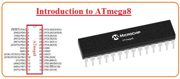
Pinout of ATmega8
- there are twenty-eight pinouts of this module which are mentioned here with the details.
PC6 (RESET)
- This is six pinouts of port C it is used as reset pinouts and also used as input and output pinouts.
- 10-bit resolution ADC
PD0 (RXD)
- It is zero pinouts of port D and used as USART serial communication interface.
- RXD (USART Input Pin)
PD1 (TXD)
- It is the first pinout of port D used as a receiver, and interrupt.
- TXD (USART Output Pin)
PD2 (INT0)
- This is the second pinout of port D which operates as an exterior interrupt.
- External Interrupt INT0
PD3 (INT1)
- It is the third pinout of port D also operates as an exterior interrupt.
- External Interrupt INT1
PD4 (XCK/T0)
- It is the fourth pinout of port D which operates as timer exterior counter input and exterior clock.
- T0( Timer0 External Counter Input)
- XCK ( USART External Clock I/O)
GND
- It is ground pinout.
PB6 (XTAL1/TOSC1)
- It is the sixth pinout of port B at this pinout external clock as input is given.
- XTAL1 (Chip Clock Oscillator pin 1 or External clock input)
- TOSC1 (Timer Oscillator pin 1)
PB7 (XTAL2/TOSC2)
- This pinout seven of port B here oscillator clock is given.
PD5 (T1)
- It is the fifth pinout of port D. here exterior counter clock is provided.
PD6 (AIN0)
- It is six pinouts of Port D here analog comparator positive is given.
PD7 (AIN1)
- it is the seventh pinout of port D which is analog comparator negative.
PB0 (ICP1)
- It is zero pinout port B which is timer pinout.
PB1 (OC1A)
- It is the first pinout of port B it is the output counter.
PB2 (SS/OC1B)
- This is the second pinout of Port B operates as SPI.
PB3 (MOSI/OC2)
- It is the third pinout of Port B which function as MOSI,
PB4 (MISO)
- This is the fourth pinout of port B and operates as MISO.
PB5 (SCK)
- It is the fifth pinout of port B and the serial clock is given here,
AVCC
- Here inner analog-to-digital converter is connected.
AREF
- This pinout is used for analog reference pinout for ADC conversion.
PC0 (ADC0)
- It is zero pinouts of port C. Here analog to digital converter channel zero is connected.
PC1 (ADC1)
- This is the first pinout of port c. Here the first channel of analog to digital converter is connected.
PC2 (ADC2)
- This second pinout of port C. Second channel of ADC connected here,
PC3 (ADC3)
- It is the third pinout of port c third channel of ADC is connected here,
PC4 (ADC4/SDA)
- It is the fourth pinout of port C fourth channel of ADC is connected.
PC5 (ADC5/SCL)
- It is the fifth pinout of port C. The Fifth channel of ADC is connected here,

ATmega8-Arduino Pin Mapping
Sleep mode of ATmega8 microcontroller
Idle Mode:
- This mode helps to stop the CPU from working and allows SPI, ADC, TWI, USART, timer, and watchdog to operate interrupt. It is configured by setting values to SM0 to SM2 bits of MCU register flags to zero.
ADC Noise Reduction Mode:
- It stops the CPU and instructs to ADC, Timer/Counter 2, external interrupt, and watchdog to operate.
Power-down mode:
- It operates external interrupts, 2 wire serial interfacing, and watchdog, and disables external oscillators and stop clocks.
Power saving mode:
- It is used for timers/counters are clocked asynchronously, and clocks except for clkASY.
Standby Mode:
- In this mode oscillator helps to work and other functions are stopped.
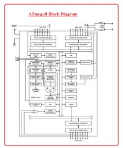
Atmega8 Microcontroller Block Figure
- 1Kbyte Internal SRAM
- 8 Kb Flash program memory
- 512 Bytes EEPROM.
I/O Ports:
- It has 3 ports B, C, and D and 23 input output lines are in these ports
Interrupts:
- 2 Exterior Interrupt in port D.
Timer/Counter:
- 3-Internal Timers, 8 bit-2, and 16 bit-1,
ADC:
- ADC (analog to digital converter) 10-bit resolution.
(SPI):
- SPI is used for serial communication protocol and pins used for this purpose are MOSI (Master Output Slave Input) and MISO (Master Input Slave Output)
USART:
- USART communication protocol is used for synchronous and asynchronous data transmission. It uses 3 pins and moslty used with PC Microcontroller.
Sleep Modes
- Power-save
- Power-down
- Standby
- Idle
- ADC Noise Reduction
Two-Wire Interface (TWI):
- It is a communication protocol that uses 2 wires for data transmission.
Applications of ATmega8
- These are some important applications of Atmega8 which are explained here.
- It is used in different control systems of industries.
- Different types of power regulation systems are employed in this module.
- For the measurement and manipulation of analog signals, this module is used.
- Different types of embedded systems use this module.
- For controlling of the motor this controller is used.
- Different types of display units are used in this module.
Faqs
What is an 8-bit AVR microcontroller?
So friends that are detailed post about ATmega8 if you have any further queries ask in the comments. Thanks for reading. Have a good day.


