 Hello, readers welcome to this engineering platform. In today’s post, we will have a detailed look at Introduction to Atmega168. It is a type of microcontroller that provides different working features and less power-consuming modules. This is AVR base controller comprises of flash memory for data storage with that it has a static random access memory unit.
In this post, we will discuss its working, features, applications, block diagram, and some other related parameters. Like other controllers, this MCU is also used in different types of control circuits and embedded projects. So let’s get started with Introduction to Atmega168.
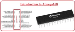
Introduction to Atmega168
- The ATmega168 is AVR-based eight-bit microcontroller that normally exist in three types of packaging configurations which are PDIP, MLF, and TQFP.
- The PDIP and MLF configuration comprises twenty pinouts and the third one TQFP is available in thirty-two pinouts.
- This module uses sixteen-kilo byte flash memory for storage of data and there is random access memory and electronically erasable program read-only memory with the space of one-kilo byte and five twelve bytes.
- In this module there are 3 types of communication protocols are used which are USAT, I2C, and serial peripheral interface.
- There is a ten-bit analog to digital converter with eight-channel assembled on this board.

Features of Atmega168
- These are some important features of this board which is described here in the details.
- There are normally twenty-eight pinouts are created at this board and in some packaging there are thirty-two pins are exist at this board.
- It comprises of eight-bit RISC-based central processing unit.
- the voltage range for which it operates is lies between 1.8 volts to 5.5 volts.
- For data storage, there is a flash memory of sixteen kilobyte.
- With flash memory, there is a random access memory of one kilobyte and an EEPROM of five twelve bytes.
- For the conversion of analog to digital converter, there is a ten-bit with eight-channel ADC is created on the board.
- One comparator for signal comparison is used at this board.
- The signal oscillator of frequency twenty megahertz is used at this board.
- There are 3 timers are exist at this board one is sixteen-bit and the other 2 is of eight bits.
- Out of twenty-eight pins twenty-three pins are used as input and output pinouts.
- It uses SPI and USART protocol for communications
- The temperature range for which it operates is lies between minus forty to plus eight five centigrade.
Pinout of ATmega168
- The main pinout of this board is described here with the details.
VCC
- At this pinout, the required voltage supply is provided to the board.
GND
- This pinout is used as ground.
Port B (PB7:0)
- This port comes in eight-bit 2D and operates as an input and output port and comprises an inner pull-up resistance.
Port C (PC5:0)
- This port is seven bits in two- dimensions and is used as input and output. It also consists of pull-up resistance.
PC6/RESET
- This pinout is operated as an input and output pinout. The electric parameters of this pinout are not alike to the other pinouts belonging to port C.
- If the RSSTDIBL fuse gets programmed, then the pinout is operated as an input and output pin, and when it gets unprogrammed, this pinout is operated as a reset pin.
Port D (PD7:0)
- This pinout is eight-bit two-dimensional and operates as an input and output port. It also comprises inner pull-up resistance.
AVCC
- This pinout is used to provide voltage to the analog-to-digital converter. In case of the absence of the operation of the analog to digital converter, this pin should be linked with the pinout VCC.
- When the analog-to-digital converter is in operating mode, this pin must link with the VCC through the low-pass filter.
AREF
- This pinout is used to provide reference analog signals to the analog-to-digital converter.
ATMEGA168 Functional Block Diagram
- The AVR comes with 32 general-purpose registers and a larger instruction set. The ALU is connected with all 32 registers. Providing 2 registers for accessing a single instruction on a clock cycle.
- The structure is effective as compared to the CISC controller, and throughput is about 10x.
- ATMEGA168 design comes with 4K/8Kbytes Read While-Write In-System Programmable Flash
- 256/512/512/1Kbytes EEPROM,
- 512/1K/1K/2Kbytes SRAM
- 23 general-purpose I/O lines
- 32 general-purpose working registers
- internal and external interrupt
- serial programmable USART
- byte-oriented 2-wire serial interface
- SPI serial port
- 3 flexible timers/counters with compare modes
- 6-channel 10-bit ADC
- CPU is off for idle mode, and SRAM, Timer USART, 2 wire interfacing, SPI, and interrupt continue working for this mode.
- The oscillator is frozen in power-down mode, off all other functions till the next interrupt reset.

Application of ATmega168
- The main application of this board is described here in detail.
- There are numerous engineering projects especially final-year projects that are used on this board.
- In robots, this board is used.
- Different types of security systems and embedded systems use these controllers.
Faqs
Is ATMEGA168 a bit chip?
- ATMEGA168-20MU is 8-bit high-performance low-power RISC-based controller that comes with 16KB ISP flash memory. 512 512B EEPROM, an 8-channel/10-bit A/D converter, and debugWIRE for on-chip debugging.
What is the difference between atmega328p and ATMEGA168?
- The basic difference is their flash features ATmega32 are 32KB and ATmega168 is 16KB.
Is ATmega a processor?
- ATMega328 is an 8-bit controller made by Atmel. It is a simple design and has features of 6PWM outputs, 6 ten-bit analog inputs, SPI, and I2C interfacing. The high speed for this module is 20MHz 5V
Is Atmel and ATmega same?
- ATmega328 is a single chip controller made by Atmel of the megaAVR family.
- It comes with a modified architecture 8-bit RISC processor core.
So friends that is a detailed post about ATmega168 I tried my level best to make simple this post for you. I hope you have understood this post if you have any further queries ask in the comments. thanks for reading. have a good day