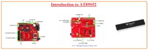
 Hello readers I hope you all are having fun in your life. In today’s post, we will have a detailed look at the introduction to AT89S52. This module belongs to the famous and most commonly used type of 8051 group of Atmel Microcontrollers. This is eight-bit and uses the CMOS technique. It comes with flash and random access memories for data storage.
The physical structure of this board is like the famous architecture of 8051 controllers. There are numerous pinouts are assembled on this controller like other microcontrollers which used to provide input to the board and get out the output from the board. In today’s post, we will have a detailed look at its working, operation, features, pinout, and some other related factors. So let’s get started with an introduction to AT89S52.
Introduction to AT89S52
- The AT89S52 is less power-consuming, highly reliable, can get data up to eight-bit, and is constructed with the CMOS (Complementary metal-oxide-semiconductor) technique.
- This module comprises of flash memory which can easily programmed and has a space of eight kilo byte.
- This controller board is created through the use of a high-density nonvolatile memory technique which is commonly used in Atmel for the construction of controllers.
- This controller also follows the different parameters set by the 80C51.
- The flash memory on this board helps the program memory to get the program after the execution of the first program through the use of non-volatile memory programming techniques.
- Through linking the eight-bit central processing unit with the flash memory over the monolithic circuit board there will be such type of controller we get that is the very powerful and less expensive and best choice for different types of embedded projects.
- With the eight-kilo byte flash memory, there is random access memory having space of two fifty-six kilobytes installed on the board.
- There are thirty-two pinouts which used as input and output is created on this board, a watchdog timer is also assembled on the board for timing processes.
- There are 2 data pointers, 3 timers of sixteen bits are used at this board.
- There are 2 modes used in this board first one is idle mode stop which controls the functions of RAM, timer, and serial port which comprises of different pinouts.
- The second mode is a power-down mode which data of random access memory.
AT89S52 Features
- The main features of AT89S52 are described here with detail.
- It comprises of eight-bit PIC central processing unit.
- There are forty pinouts including inputs and output pinouts are created on this board.
- The voltage range over which it can run is from four volts to 5.5 volts.
- There are thirty-two pinouts out of forty which can be reprogrammed.
- Like other controllers, it does not comprise an analog-to-digital converter.
- There is one sixteen-bit timer is created on this board.
- It does not also have a comparator.
- There are no digital-to-analog converter exits in this controller.
- It uses the UART protocol for communications.
- It comprises the exterior oscillator having a frequency of twenty-three megahertz.
- There are no inner oscillator exits on this controller.
- It has programmable flash memory. The size of this memory unit is an eight-kilo byte.
- The RAM of two fifty-six bytes is created at this device.
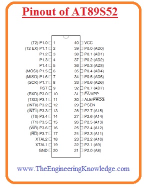
Pinout of AT89S52
P1.0 (T2)
- This pinout belongs to the first port and it is zero general input and output pinout of this port.
P1.1(T2.EX)
- It is the first pinout of port one and used as a counter.
P1.2
- This is the second pinout of port one.
P1.3
- This is the third general-purpose pinout of port one.
P1.4
- This is the fourth pinout of the first port.
P1.5 (MOSI)
- This pinout is belonged to the port one and uses as a master out slave in pinout.
P1.6 (MISO)
- This is the sixth pinout of port one and used as a master in slave out.
P1.7 (SCK)
- This is the seventh pinout of port one and a serial clock is provided at this pinout.
RST
- This is reset pinout and reset the controller.
P3.0 (RXD)
- This is zero general-purpose pinouts of port three and used as serial receiver input pinout.
P3.1 (TXD)
- It is the first pinout of port three and used as a serial transmitter pinout.
P3.2 (INT0)
- This is the second pinout of port three here exterior interrupt zero is provided.
P3.3 (INT1)
- This is the third general-purpose pinout of port three here outer interrupt one is provided.
P3.4 (T0)
- This fourth general-purpose pinout of third port and here zero timers is provided.
P3.5 (T1)
- This is the fifth pinout of port three here timer one is attached.
P3.6 (WR)
- It is the sixth pinout of port three and used for the writing of memory.
P3.7 (RD)
- It is the seventh pinout of the third pinout and is used for reading of the memory.
XTAL2
- At this pinout, the outer oscillator output is connected.
XTAL1
- Here exterior oscillator input is provided.
GND
- This pinout is the ground pin of the controller.
P2.0(A8)
- This zero pinout off port two.
P2.1 (A9)
- This is the first pinout of second port.
P2.2 (A10)
- This is the second pinout of the second port.
P2.3 (A11)
- This is third pinout of port two.
P2.4 (A12)
- This is the fourth pinout of port two.
P2.5 (A13)
- This is the fifth pinout of the second port.
P2.6 (A14)
- This is the sixth pin0ut of port two.
P2.7 (A15)
- This is the seventh pinout of the second port.
PSEN’
- This pinout helps to read the outer program memory.
ALE / PROG
- This pinout is used to enable the latch address.
EA’ / VPP
- This is pinout to enable the outer access.
P0.7 (AD7)
- This is the seventh pinout of port zero and is used for data addressing.
P0.6 (AD6)
- This is the sixth pinout of zero port.
P0.5 (AD5)
- This fifth pinout of port zero and used for transmission of data.
P0.4 (AD4)
- This is the fourth pinout of port zero.
P0.3 (AD3)
- This is the third pinout of the zero port and is used as a data pinout.
P0.2 (AD2)
- This is the second pinout of the zero port and used as a data pin.
P0.1 (AD1)
- This is first pinout of zero port and operates as data pinout.
0 (AD0)
- This is zero pinout of port zero.
VCC
- At this pinout plus five volts are provided.
Application of AT89S52
- This module is used in different types of DIY projects.
- For a proper understanding of Atmel, this board can help you.
- Due to the large number of pinouts, it is mostly preferred for such projects where many devices are assembled.
- It can be used in place of Arduino.
- It is also used in automobile, industries, and different types of analog-to-digital converter
Faqs
What is the description of microcontroller AT89S52 pin?
- This controller comes with GPIO pins three are 16 bits timers, a full-duplex UART communication port, etc. With that, it has 40 pins, 32 are GPIO pins and AT89S52 comes with an inbuilt watchdog timer for working to low power mode.
What is the function of AT89S52?
- AT89S52 is low power, CMOS 8-bit controller having 8K bytes for in-system programmable flash memory.
- It is made with the use of a high-density nonvolatile memory system and supports standard 80C51 instruction set and pinout.
What is the difference between 89c52 and 89s52?
- AT89C52 does not support serail programming and AT89S5 compatible with serial and parallel programming.
What is the difference between AT89C51 and AT89C52?
- The basic difference is that controllers are RAM and flash memory. All come with the same pin and fewer differences they have 89c5comes with 128 bytes of ram and 89c52 has 256 bytes.
What are the specifications of AT89S52?
| Program Memory Size (KB) | 8 |
| Pin Count | 44 |
| Operation Voltage Max.(V) | 5.5 |
| Operation Voltage Min.(V) | 4 |
| ADC Resolution Max | 0 |
What does the S in at89s51 indicate?
- S is standard Vcc voltage schottky
What are the features of an 8051 microcontroller?
- 4KB bytes on-chip program memory (ROM)
- 8-bit bidirectional data bus.
- 16-bit unidirectional address bus.
- 32 general purpose registers each of 8-bit.
- 16-bit Timers
- 128 bytes on-chip data memory (RAM)
- 4 register banks.
- 128 user-defined software flags.
Read also:
That is a detailed post about AT9S52 if you have any queries ask in the comments. Thanks for reading.


