 Hello, readers welcome to the new post. Today we will discuss How to Make PCB Panels. For the design of a PCB board, the important fact is the layout of a board that helps to position the components traces and holes drilling on the board. Another point is features of layout, and clearance of edge for board calculate PCB panelization during manufacturing and assembly.
The creation of PCB panels is a very effective way to make more boards of similar designs in groups and a combination of more boards called PCB panels and the creation of this group is called PCB panelization. In this post, we will have a detailed look at PCB panels and tell you how you can make panels from PCBWAY.
What is PCB Panelization?
- Sometimes you create PCB board from your manufacturer that comes in single units but these boards are created in larger groups that have more units in the panel
- In the below figure you can see that same unit of board in the panel.
- The panelization process of PCB is effective in the creation of a single unit it is also cost-efficient.
- The process through which boards are separated from panels is called depanelization. When depanelizton did some waste is produced that relies on the quantity of board in the panel and depanelization techniques

PCB Depanelization Methods
- There are 2 techniques used for depanlization first one is routing and the second one is scoring. These two methods can be applied together or singly based on board design weight, direction and soldering methods.
Routing
- It is used for older categories of the board and in this method router bit is used to make holes for PCB separation.
Scoring
- In this technique, V-shaped groove is used to cut board thickness 1/3 from the upper to the lower part
Importance of PCB Panel
- The creation of PCB panel enhances the SMT assembly technique efficiency. If the panel has a larger number of boards less time will be for one PCB to send and operate in hub and pasting devices used will have a high rate that in a result increases the SMT efficiency
- Panleization process also improves SMT production to avoid different issues during the manufacturing process. The distribution density of PCB components is large, some components such as the outline of the edge connectors may be beyond the edge of the PCB, before reflow soldering and wave soldering are completed, all these components are removable, so you need to have additional breakout bars and increase the area of the whole panel to these peripheral components were prevented from being affected by external factors and the assembly quality was reduced.
- The panel is also designed to facilitate the operation of the production line. PCB assembly has to go through many steps. Finished PCBs or semi-finished PCBs should be put into a rotary box, and these PCBs would be moved, stored and transported by a rotary rack. These operations require a specific process edge to prevent damage to the component on the printed circuit board.
Types of Panel Design
- It does not need to take tension about the type of PCB board there is a certain structure of panel followed by the PCB. There are different techniques used for panelization.
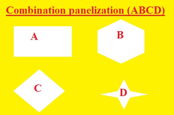
- Different design configurations are used for PCB panels like AAAA, ABAb or ABCD. It is not easy to generalize which type of panel is good, which needs to be determined by considering the density and layout of the components on the board as well as the device configuration. All these types of panels have their advantages and disadvantages.
penalization (AAAA) Combination
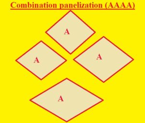
- AAAA combination of panelization is mostly used. There are different benefits of this combination.
- This combination is compatible with every type of MST process technique and not special measures are taken
- Second, paneling ordering is not affected by production numbers, permitting the highest quantity of panels to be effective based on the maximum number of SMT components to result in the highest manufacturability of all paneling combinations.
- Third, the print quality will not be reduced due to the pad orientation of the special components in the printing template design process.
- At last operational difficulties will not accumulate due to different panel orientations in each run of the entire process
Combination panelization (ABCD)
- There are some advantages of this combination of panelization.
- It is a good option for a production model containing multiple combinations of PCBs in products such as household appliances and toys
- .Second, it is beneficial to improve production efficiency and reduce costs, so product turnover and blank inventory can be greatly reduced, which can meet customers’ requirements for fast transportation.
- It also has some drawbacks. On the one hand, it is difficult to control product differentiation in the assembly line process, which leads to product chaos. Firstly, when one panel in the combination suffers from poor quality or even waste, the total number of penalizations will decrease, and it is bad for production rehabilitation.
- On the other hand, when one panel in combination has poor quality or even waste, the total number of penalizations will decrease, and it is bad for production rehabilitation.
How to Make PCB Panel
- There are different PCB suppliers are working and offering PCB-based services. PCBWAY is a China-based PCB supplier that offers different PCB services like different types of PCBs, PCBA, and some other related services.
- Their business goal is to be the most professional prototyping and small-batch PCB manufacturer in the world. With more than a decade in the industry, they are committed to meeting the needs of our customers from various industries in terms of quality, delivery, economy, and any other demanding requirements. As one of the most experienced PCB and SMT Assembler manufacturers in China, they are proud to be your best business partners as well as good friends in every aspect of your PCB needs. they strive to make your R&D work easy and hassle-free.
- With providing high-quality PCB services from PCBWAY you can get PCB panel services with high quality and affordable prices.
- To get the PCB panels from PCBWAY visit their site.
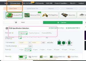
- Here you can see the PCB instant quote press on it and PCB Specification Selection interface will open that can seen here.
- In this interface, you can see two options Panel by customer and panel by PCBWAY select these options according to your requirements.
- When you select the PCB panel options then put other parameters of your board and place an order.
- Their engineers will review your order details and after making sure all details start creation and update you about your products.’
- Through using their customer services you can get the details of your products at any instant
Factors that Affect Panel Cost
- Substrate cost: For the sample order, we use PCBWay as the default, if the panel size is smaller than 100*100mm and should not contain the number of individual PCBs exceeding 10 pieces. For example, if a customer places a sample order, they require that the panel size is 100x100mm, but the panel includes 14 separate plates, then we need to charge the substrate fee and the filming fee.
- Several drilling holes: If customers want more drilling holes than our specified quantity they have to pay extra. For instance, we offer 500 holes for each 100 by 100mm dimension and if you need more holes then you have to pay extra cost
- Number of V-cutting: If you need more V-cutting then you have to pay the PCBWAY mentioned prices. For instance, They have the default number of V cutting not larger than ten for 100 by 100mm dimensions s and if you need more then you have to pay extra
- Electrical Tests: Different products need different testing techniques so prices will be according to tests
- Emergency Charges: Usually PCBWAY delivers an order in three days but if you need urgent delivery have to pay extra
That is all about the How to Make PCB Panel all details have been explained if you have any questions ask them here.
Read also
- WHAT IS PCB Panelization
- What is Ball Grid Array (BGA) on a PCB Board
- Introduction to 3D PCB Boards & Advantages
- How to Get High Quality and Low Cost PCB Board
- What is Polyimide PCB Board
