

 Hello fellows, I hope you all are doing great. In today’s tutorial, we will have a look at How Circuit Capacitances Affect Frequency Response of Amplifier. In amplifier circuits coupling and bypass, capacitors look short to ac at midband frequencies (MidBand frequency or sub-6 is spectrum used for wireless data transmission. It works among the one and six Gigahertz frequencies). For less frequency capacitive reactance of these capacitors disturbs the gain and phase shift of signals therefore they are taken into consideration.
The variation in gain or phase shift for a certain value of input signal frequency is known as frequency response. In today’s post, we will have a detailed look at the capacitive effect of capacitors on frequency response used in amplifiers. So let’s get started with how circuit capacitances affect frequency response of an amplifier.
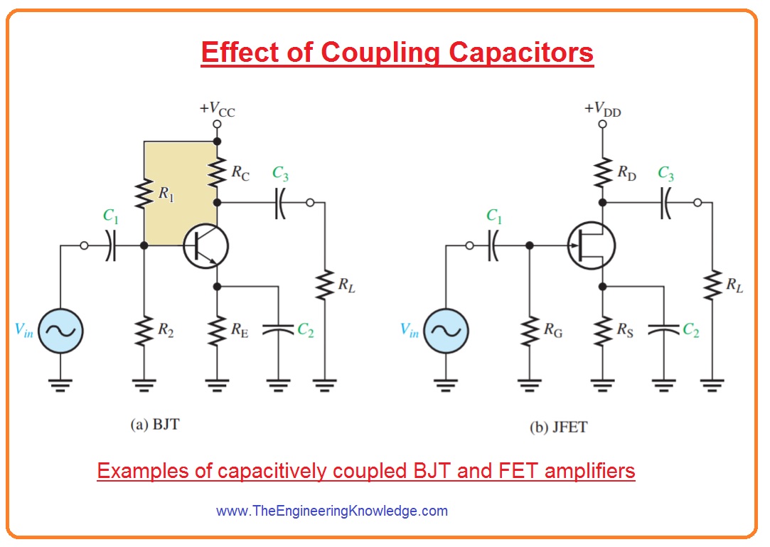
Effect of Coupling Capacitors
- As we are aware of this basic equation XC=1/2πfc it indicates that there is an inverse relationship between capacitive reactance and frequency.
- For less frequency reactance is larger and reduces with the increment in frequency.
- For less frequency, for instance, audible frequency less than ten hertz capacitively coupled amplifier as shown in below figure has low voltage gain it has at high frequency.
- The cause is that for less frequency larger voltage loss about capacitors C1 and C3 occurs since their reactance is larger.
- The large voltage loss at less frequency decreases the voltage gain.
- With that phase shift is presented with the coupling capacitors since capacitor C1 makes a lead circuitry with the Rin of amplifier and capacitor C3 make lead circuitry with the resistance RL in series with the RC or RD.
- The lead circuit is RC circuitry which has output voltage about R leading input voltage in phase.
Effect of Bypass Capacitors
- At less frequency value the reactance of bypass capacitor denoted as C2 in above figure becomes important and the emitter is not now at ac ground.
- The capacitive reactance XC2 is in parallel with resistance RE that make an impedance which decreases the gain. It explained in below figure.
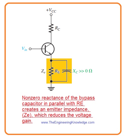
- For instance when the value of frequency is large and value of voltage of common emitter amplifier is Av= RC/r’e.
- For less value of frequency XC>>0 ohm and voltage gain is Av= RC/ (r’e + Ze).
Effect of Internal Transistor Capacitances
- For large frequency the coupling and bypass capacitors behaves like ac shorts and has no effect on the amplifier’s response.
- Inner transistor junction capacitance, though, do come into play, dropping an gain of amplifier and causes phase shift as signal frequency rises.
- The below figure shoes inner pn junction capacitances for both BJT and JFET transistors.
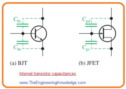
- For bipolar junction transistor Cbe is the base emitter junction capacitance and Cbc is base collector junction capacitance.
- While for JFET Cgs is capacitance among gate and source and Cgd is the capacitance among gate and drain.
- Datasheets frequently denote to the BJT capacitance Cbc as the output capacitance, frequently nominated Cob.
- The capacitance Cbe is frequently denoted as the input capacitance Cib.
- The Datasheets of field effect transistors usually denoted input capacitance Ciss and reverse transfer capacitance Crss.
- From these parameters Cgs and Cgd can be measured.
- For less frequency the inner capacitance has large reactance since of their less capacitance value and less frequency value.
- So, they appear like open circuit and have no effect on the working of transistor.
- With the increment in frequency the inner capacitive decrease and at certain point have effect on the gain of transistor.
- When the reactance of Cbe is less enough the sufficient quantity of signal voltage is losses due to voltage divider effect signal source resistance and reactance of Cbe. It is explained in below figure denoted as ‘a’.
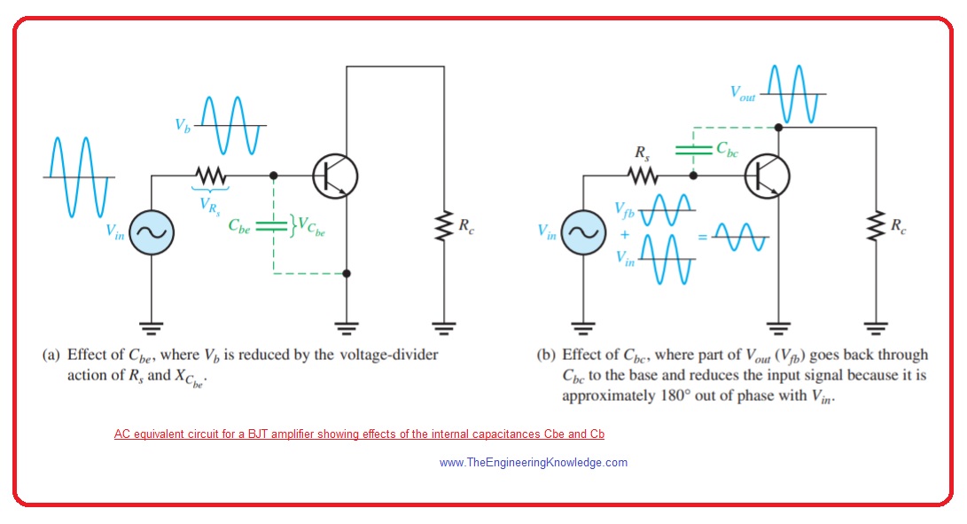
- When reactance Cbe is less enough a certain quantity of output signal voltage is fed back out of phase with the input. hence, efficiently dropping the voltage gain. It explained In above figure denoted as ‘b’.
Miller’s Theorem
- Miller theorem is applied to make simple analysis of inverting amplifiers at large frequency where inner transistor capacitances are significant.
- The capacitance Cbc in bipolar junction transistor or Cgd for field effect transistor among the input and output is shown in below figure denoted as ‘a’.

- The Av is absolute voltage gain of inverting amplifier for midrange frequency values and C denoted Cbc or Cgd.
- Miller theorem explains that C looks as capacitance from input ot ground as shown in above figure denoted as ‘b’ it can define as.
Cin(Miller)=C(Av +1)
- This equation indicates that Cbc has larger impact on input capacitance than its real value.
- For instance if Cbc is sic picofarad and gain of amplifier is fifty then will be Cin(Miller) 306 picofarad.
- The below figure indicates that how this effective input capacitance look in the real ac resultant circuitry in parallel combination with the Cbe.
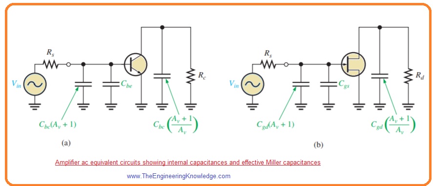
- Miller theorem also says that C looks as capacitance from output to ground and can be defined as.
Cout(Miller)=C((Av+1)/Av)
- This equation shows that if voltage gain is ten or larger Cout(Miller) is almost equal to the Cbc or Cgd since (Av +1)/Av is almost equal to one.
- Above figure also explains how this output capacitance looks in the ac resultant circuitry for BJT and FET.
That is detailed post about Circuit Capacitances Affect Frequency Response of Amplifier if you have any question ask in comments. Thanks for reading.