
 Hello, friends, I hope you all are doing great. In today’s tutorial, we will discuss the Difference Between NPN vs PNP Transistors. The basic difference between NPN and PNP transistors is that in an NPN transistor current moves from the collector to emitter after the application of positive supply to the base while in PNP configuration the current flow emitter to the collector after the application of negative supply at the base terminal. Both NPN and PNP are types of BJT or bipolar junction transistors. It is a device used to regulate the current and can also use as a switch or amplifier.
In mostly circuitry NPN transistor is used since in NPN transistor current flows due to electrons while in PNP transistor current flows due to holes. Due to the fast movement of electrons, high conduction occurs in the NPN. In today’s post, we will have a detailed look at both NPN and PNP transistors with the details and compare them to find their differences. So let’s get started with Difference Between NPN vs PNP Transistors.
Difference Between NPN vs PNP Transistor
NPN Transistor
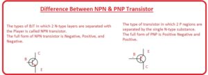
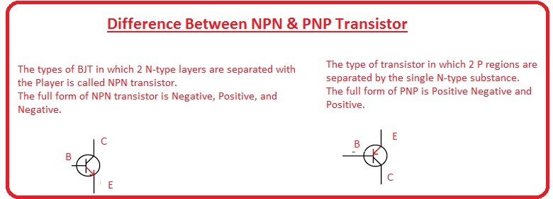
- The types of BJT in which 2 N-type layers are separated with the Player is called NPN transistor.
- The full form of the NPN transistor is Negative, Positive, and Negative.
- Its switching speed is high than the PNP.
- The minority carriers in this transistor are holes.
- The positive voltage is given at the collector of the NPN transistor.
- The direction of current flow in the NPN transistor is from Collector to Emitter.
- Its starts operation after entering of electrons in the base.
- In this transistor current is generated due to the movement of electrons.
- Its outer side current is generated due to the movement of holes.
- In this transistor majority, charge carriers are electrons.
- Its emitter-based junction is a forward-biased state.
- The collector-base junction is reverse-biased.
- Less value of current flows from emitter-to-base.
PNP Transistor
- The type of transistor in which 2 P regions are separated by the single N-type substance.
- The full form of PNP is Positive Negative and Positive.
- It starts operation after the entrance of holes in the base.
- Its inner current is generated due to the movement of holes.
- Its outer current generates due to the movement of electrons.
- Its switching speed is less than the NPN transistor.
- In this transistor, electrons are minority charge carriers.
- The voltage is given to the emitter of the transistor.
- The direction of the current flow in this transistor is from Emitter to Collector.
- Its Emitter Base Junction is forward biased state.
- Its Collector Base Junction is a reversed-biased state.
- A small value of current flows from base to emitter.
NPN vs PNP Transistor
Here some points for NPN vs PNP Transistor explained
| Feature | NPN Transistor | PNP Transistor |
|---|---|---|
| Structure | It comes with a sandwich-like structure with a P base and N emitter and a collector | It have N sandwiched between the collector and emitter which are P-type materials |
| Current carriers | Electrons | Holes |
| Majority carriers | Electrons | Holes |
| Minority carriers | Holes | Electrons |
| Polarity | (NPN) or Negative-positive-negative | Positive-negative-positive or (PNP) |
| Voltage polarity | The collector is positive relative to the emitter | The emitter is positive relative to the collector |
| Biasing | Forward-biased base-emitter junction and reverse-biased base-collector junction | Forward-biased base-collector junction and the reverse-biased base-emitter junction |
| Operation | In an NPN transistor, a small current passes through the base to cause a larger current from the collector to the emitter | In a PNP transistor, a small current flowing out of the base that allows a larger current to flow from the emitter to the collector. |
| Current amplification | It has High current amplification | Amplification low current |
| Voltage gain | Good voltage gain | Poor voltage gain |
| Power handling | Lower power handling capability | Higher power handling capability |
| Output signal | Inverted output signal | Non-inverted output signal |
| Input impedance | High input impedance | Low input impedance |
| Output impedance | Low output impedance | High output impedance |
| Noise | Low noise | High noise |
| Speed | Fast switching speed | Slow switching speed |
| Temperature sensitivity | Less sensitive to temperature changes | More sensitive to temperature changes |
| Saturation voltage | 0.7 V | -0.7 V |
| Cost | Less expensive | Costly |
| Applications | Amplifiers, switches, and digital circuits | Amplifiers, switches, and digital circuits |
| Common-emitter configuration | Most commonly used configuration | Less commonly used configuration |
| Common-collector configuration | Used as voltage followers or impedance-matching circuits | Used as current amplifiers or switches |
| Common-base configuration | Employed in high-frequency applications | Employed in low-frequency applications |
| Maximum frequency | It has a maximum frequency | It has a maximum frequency |
| Leakage current | It has high leakage current | Less leakage current |
| Reverse breakdown voltage | Lower reverse breakdown voltage | Higher reverse breakdown voltage |
| Power efficiency | Low power efficient | High power efficient |
Types of Transistors & BJT VS FET / MOSFET
| Transistor Type | Structure | Operation | Current Carriers | Voltage Gain | Power Handling | Input Impedance | Output Impedance | Noise | Speed | Temperature Sensitivity | Saturation Voltage | Cost | Applications |
|---|---|---|---|---|---|---|---|---|---|---|---|---|---|
| BJT | Sandwich-like structure with p-type or n-type base, an n-type or p-type emitter and collector regions | Current flow from emitter to collector is controlled by a small current into the base | Electrons and holes | Good voltage gain | Lower power handling capability | High input impedance | Low output impedance | Low noise | Fast switching speed | More sensitive to temperature changes | 0.7 V (NPN), -0.7 V (PNP) | Inexpensive | Amplifiers, switches, and digital circuits |
| FET/MOSFET | Gate is separated from the channel by an insulating layer, and the gate voltage controls the current flow through the channel | Current flow through the channel is controlled by the voltage applied to the gate | Majority carriers (either electrons or holes, depending on the type of FET) | Poor voltage gain | Higher power handling capability | Low input impedance | High output impedance | Low noise | Slow switching speed | Less sensitive to temperature changes | No saturation voltage | More expensive | Amplifiers, switches, and digital circuits |
FAQS
- Write the difference between an NPN and PNP transistor.
- The basic difference between NPN and PNP transistors is their charge carriers that are sued to carry current. In NPN electrons are the majority carriers and PNPN has holes as the majority carriers.
- Write the main applications of NPN and PNP transistors.
- The main applications of NPN and PNP are digital circuits, amplifiers, voltage regulators, and motor control circuits
- Which transistor has a high input impedance value?
- The input impedance of PNP transistors is high than NPN
- Which transistor has a high output value of impedance?
- NPN has high output impedance
- Write the main purpose of a transistor.
- The transistor is semiconductors components used for amplification or switching circuits. It is mostly used in radio, tv computers, and other electronic devices
That is a detailed post about the difference between NPN vs PNP transistors if you have any queries ask in the comments. Thanks for reading. Have a good day.