 Hello, readers welcome to the new post. Here we will discuss Difference Between Intrinsic and Extrinsic Semiconductors. the basic difference between these two is their doping level, holes, and electron quantity define their differences.
Here we will cover all details about these materials. So let’s get started.
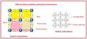
Difference Between Intrinsic and Extrinsic Semiconductor
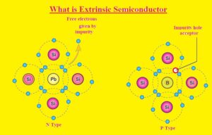
What is Extrinsic Semiconductor
- These semiconductors are created if the impurity is added in the intrinsic semiconductors. That is called a doped or impurity semiconductor
- Semiconductors are such material that has conductivity among the conductor and insulator called amorphous solids.
- The addition of doped or impurity material enhances its electric features and is used in different electronic devices such as transistors and diodes
- Doping is a technique through which bandgap is regulated through the addition of impurity substances.
- The addition of other materials to a semiconductor enhances its conductance multiple times the added materials called dopants
- The impurity material added depends on the final semiconductors obtained.
- A decent extrinsic semiconductor can be created by adding a small amount of impurity.
- Before adding the impurity make sure that the dopant is the same size to the original atom also dopants not disturb the structure of the original atom
Types of Dopants in Extrinsic Semiconductors
- Doping results to vary the conduction in semiconductors. The components of 4th group of the periodic table such as silicon and germanium known as semiconductors these two materials have tetravalent crystals so used for 2 categories of dopants
- P-type semiconductor
- N-type semiconductor
- A diode is a semiconductor device that used in circuits as rectifier
- P and N materials combine to make the PN junction
- These devices are used in FET and BJT.
- It used as a switches
- Doping does not vary the net neutrality of component
- Electrons are the majority in N semiconductors and holes in P semiconductors
What is Intrinsic Semiconductor
- The semiconductors that are not doped are called intrinsic or pure semiconductors. The charger carries through finding the features of material in place of impurity added like extrinsic material
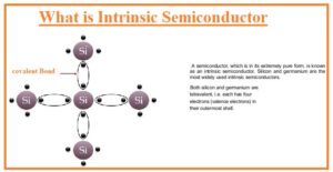
- These materials have the same electrons and holes.
- The conduction of material can be affected through crystallographic causes of technology
- In this material such as silicon over a temperature value larger than the absolute zero gets energy and moves from the excitation to the conduction band resulting in a current
- When electrons change the band holes are created at their place. Due to external forces applied by the volts electrons and hoes move in the substances.
- In the case of N, material impurity gives additional electrons that enhance the conductivity
- In case of P-type material dopant generates additional holes also increases the conduction,
What is Semocinductior Current
- The current flowing in the intrinsic material is caused by both holes and electron currents.
- Electrons that are released from the conduct in the conduction band can move in the substances.
- As a result, other electrons come to fill the position created by the released electrons
- This process is known as hole conduction since it is created as if holes are moving in the substance against the direction of electrons.
- The current flowing through these materials is affected by the energy states that have an impact on the quantity of the electrons in the conduction band, SO can say that this current relies on the temperature
FAQs
What are N type and P-type semiconductors?
- P-type semiconductor is made with group III components doping, such as Boron, aluminum, and Thallium. N-type semiconductor is made with group V elements Nitrogen, Phosphorus, etc. They are called trivalent semiconductors and also N-type called pentavalent semiconductors.
What is an example of an extrinsic semiconductor?
- The basic examples of extrinsic semiconductors are silicon doped with boron. Boron comes with one electron less than silicon and when added to silicon lattice makes extra holes that work as positive charge carriers. As a result, make P-type
What is the forbidden energy gap?
- The forbidden gap is the space between the valence band and the conduction band. In this gap, there is no energy and no electron in this band.
What is an extrinsic semiconductor in simple terms?
- Extrinsic semiconductor is material that has doping of some impurities. The impurities affect the electrical features of semiconductors and are best for devices to be used in diodes and transistors.
Why is silicon preferred over germanium?
- The main cause for choosing silicon then germanium is the best thermal stability. It is due to the high melting point that helps to work in good condition. Germanium comes with good electrical conductivity and its insulating features make it best for use in electronic devices.
Read also
That is all about the Difference Between Intrinsic and Extrinsic Semiconductor. all details has been explained. If you have any further queries ask in comments. Thanks for reading have a nice day.


1 Comment